LD1117AV View Datasheet(PDF) - STMicroelectronics
Part Name
Description
Manufacturer
LD1117AV Datasheet PDF : 16 Pages
| |||
LD1117A SERIES
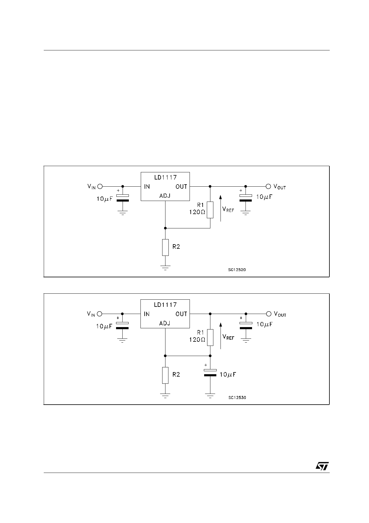
LD1117A ADJUSTABLE: APPLICATION NOTE
The LD1117A ADJUSTABLE has a thermal stabilized 1.25±0.012V reference voltage between the OUT
and ADJ pins. IADJ is 60µA typ. (120µA max.) and ∆IADJ is 1µA typ. (5µA max.).
R1 is normally fixed to 120Ω. From figure 7 we obtain:
VOUT = VREF + R2 (IADJ + IR1) = VREF + R2 (IADJ +VREF /R1) = VREF (1 + R2 / R1) + R2 x IADJ.
In normal application R2 value is in the range of few Kohm, so the R2 x IDJ product could not be
considered in the VOUT calculation; then the above expression becomes:
VOUT = VREF (1 + R2 / R1).
In order to have the better load regulation it is important to realize a good Kelvin connection of R1 and R2
resistors. In particular R1 connection must be realized very close to OUT and ADJ pin, while R2 ground
connection must be placed as near as possible to the negative Load pin. Ripple rejection can be improved
by introducing a 10µF electrolytic capacitor placed in parallel to the R2 resistor (see Fig.8).
Figure 7 : Adjustable Output Voltage Application
Figure 8 : Adjustable Output Voltage Application with improved Ripple Rejection
10/16
Share Link: 