MAX8640Z(2007-07) View Datasheet(PDF) - Maxim Integrated
Part Name
Description
Manufacturer
MAX8640Z Datasheet PDF : 11 Pages
| |||
Tiny 500mA, 4MHz/2MHz Synchronous
Step-Down DC-DC Converters
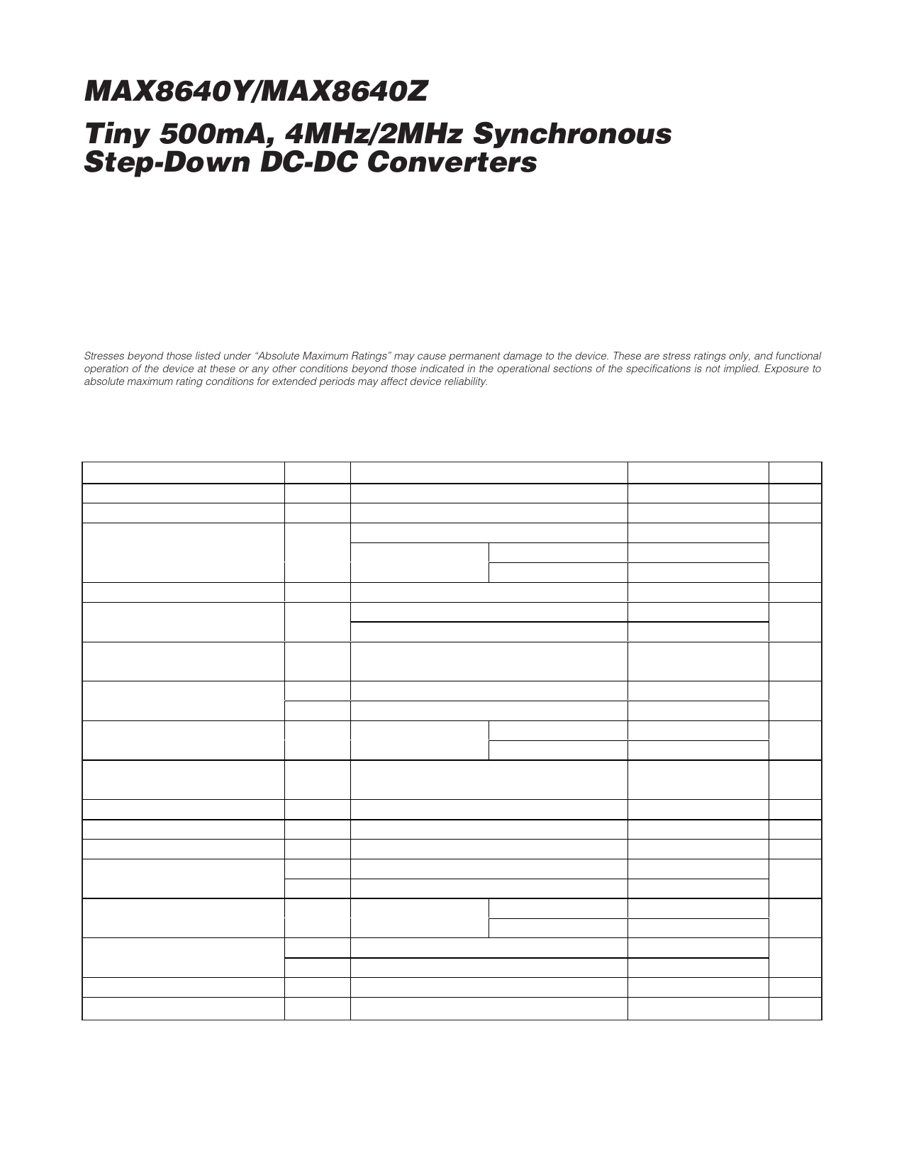
ABSOLUTE MAXIMUM RATINGS
IN to GND .................................................................-0.3V to +6V
LX, OUT, SHDN to GND ..............................-0.3V to (VIN + 0.3V)
LX Current (Note 1) ........................................................0.8ARMS
OUTPUT Short Circuit to GND ...................................Continuous
Continuous Power Dissipation (TA = +70°C)
6-Pin SC70 (derate 3.1mW/°C above +70°C) ..............245mW
6-Pin µDFN (derate 2.1mW/°C above +70°C) ..............167.7mW
Operating Temperature Range ...........................-40°C to +85°C
Junction Temperature ......................................................+150°C
Storage Temperature Range .............................-65°C to +150°C
Lead Temperature (soldering, 10s) .................................+300°C
Note 1: LX has internal clamp diodes to IN and GND. Applications that forward bias these diodes should not exceed the IC’s package
power-dissipation limit.
Stresses beyond those listed under “Absolute Maximum Ratings” may cause permanent damage to the device. These are stress ratings only, and functional
operation of the device at these or any other conditions beyond those indicated in the operational sections of the specifications is not implied. Exposure to
absolute maximum rating conditions for extended periods may affect device reliability.
ELECTRICAL CHARACTERISTICS
(VIN = 3.6V, SHDN = IN, TA = -40°C to +85°C, typical values are at TA = +25°C, unless otherwise noted.) (Note 2)
PARAMETER
SYMBOL
CONDITIONS
MIN TYP
Supply Range
UVLO Threshold
VIN
UVLO
VIN rising, 100mV hysteresis
No load, no switching
2.7
2.44 2.6
24
Supply Current
Output Voltage Range
Output Voltage Accuracy
(Falling Edge)
ICC
VOUT
SHDN = GND
TA = +25°C
TA = +85°C
Factory preset
ILOAD = 0mA, TA = +25°C
ILOAD = 0mA, TA = -40°C to +85°C
0.01
0.1
0.8
-1
0
-2
Output Load Regulation
(Voltage Positioning)
Equal to inductor DC resistance
RL
SHDN Logic Input Level
SHDN Logic Input Bias Current
Peak Current Limit
Valley Current Limit
Rectifier Off-Current Threshold
On-Resistance
LX Leakage Current
Minimum On and Off Times
Thermal Shutdown
VIH
VIL
IIH,IL
ILIMP
ILIMN
ILXOFF
RONP
RONN
ILXLKG
tON(MIN)
tOFF(MIN)
VIN = 2.7V to 4.9V
VIN = 2.7V to 4.9V
VIN = 4.9V,
SHDN = GND or IN
TA = +25°C
TA = +85°C
pFET switch
nFET rectifier
nFET rectifier
pFET switch, ILX = -40mA
nFET rectifier, ILX = 40mA
VIN = 4.9V, LX = GND TA = +25°C
to IN, SHDN = GND
TA = +85°C
1.4
0.001
0.01
590 770
450 650
10
40
0.6
0.35
0.1
1
95
95
+160
Thermal-Shutdown Hysteresis
20
MAX
4.9
2.70
48
0.1
2.5
+1
+2
0.4
1
1400
1300
70
1.2
0.7
1
UNITS
V
V
µA
V
%
V/A
V
µA
mA
mA
mA
Ω
µA
ns
°C
°C
Note 2: All devices are 100% production tested at TA = +25°C. Limits over the operating temperature range are guaranteed by design.
2 _______________________________________________________________________________________
Share Link: 