MAX9546(2005) View Datasheet(PDF) - Maxim Integrated
Part Name
Description
Manufacturer
MAX9546 Datasheet PDF : 12 Pages
| |||
Differential Video Interface Chipset
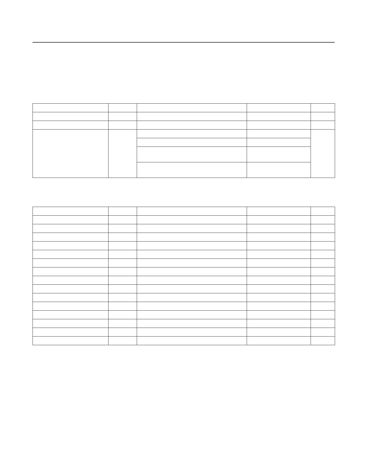
AC ELECTRICAL CHARACTERISTICS—MAX9547
(VCC = +8.5V, GND = 0V, RL = 75Ω, ZZT = 75Ω, CL = 50pF, TA = -40°C to +85°C, Typical values are at TA = +25°C.) (Note 2)
PARAMETER
Large-Signal Bandwidth
Large-Signal Flatness
Slew Rate
Settling Time (0.1%)
Power-Supply Rejection Ratio
Common-Mode Rejection Ratio
LOS Timeout Period
SYMBOL
SR
tSETTLING
PSRR
CMRR
tLOS
CONDITIONS
VIN = 1VP-P, -3dB
VIN = 1VP-P, ±0.5dB
f = 100kHz, 100mVP-P ripple
f = 100kHz, 100mVP-P ripple
MIN TYP MAX UNITS
20
MHz
15
MHz
50
V/µs
400
ns
30
dB
53
dB
760
µs
AC ELECTRICAL CHARACTERISTICS—MAX9546 Driving MAX9547
(VCC = +8.5V, RL = 220Ω across OUT+ and OUT-, RL = 75Ω (MAX9547), ZZT = 75Ω, TA = -40°C to +85°C. Typical values are at TA =
+25°C, unless otherwise noted.) (Note 2)
PARAMETER
Differential Gain
Differential Phase
Signal-to-Noise Ratio
SYMBOL
DG
DP
SNR
CONDITIONS
5MHz lowpass, 100kHz highpass,
VIN = 1VP-P
MIN TYP MAX UNITS
3.8
%
0.6
degrees
80
dB
2T Pulse-to-Bar Rating
2T = 250ns, bar time is 18µs, the beginning
3.5% and the ending 3.5% of the bar time is
0.2
%
ignored
2T Pulse Response
Group Delay
2T = 250ns
D/dt At 3.58MHz
0.25
%
10
ns
Note 2: All devices are 100% production tested at TA = +25°C. All temperature limits are guaranteed by design.
Note 3: Defined as differential output to single-ended input.
Note 4: Input is AC-coupled.
Note 5: The RC time constant (3Hz) formed by the source resistance (RS) and coupling capacitor (CIN) is usually used for lead
compensation of the active clamp. The source resistance is 400Ω max. The clamp should remain stable in this condition.
Note 6: Differential mode is defined as (OUT+ - OUT-). Common mode is defined as OUT+ + OUT-
2
Note 7: A fault is when the outputs both sink and source current and the amount of extra current sink or source is greater than 3mA.
Note 8: Common-mode balance is defined as 20log((OUT+ - OUT-) / (OUT+ + OUT-)).
Note 9: Ground between MAX9546 and MAX9547 can be a ±2V difference.
Note 10: A loss-of-signal is when the input video signal of the MAX9547 does not change (cross 100mV level from sync tip) for 10
video lines.
4 _______________________________________________________________________________________
Share Link: 