MAX9546(2005) View Datasheet(PDF) - Maxim Integrated
Part Name
Description
Manufacturer
MAX9546 Datasheet PDF : 12 Pages
| |||
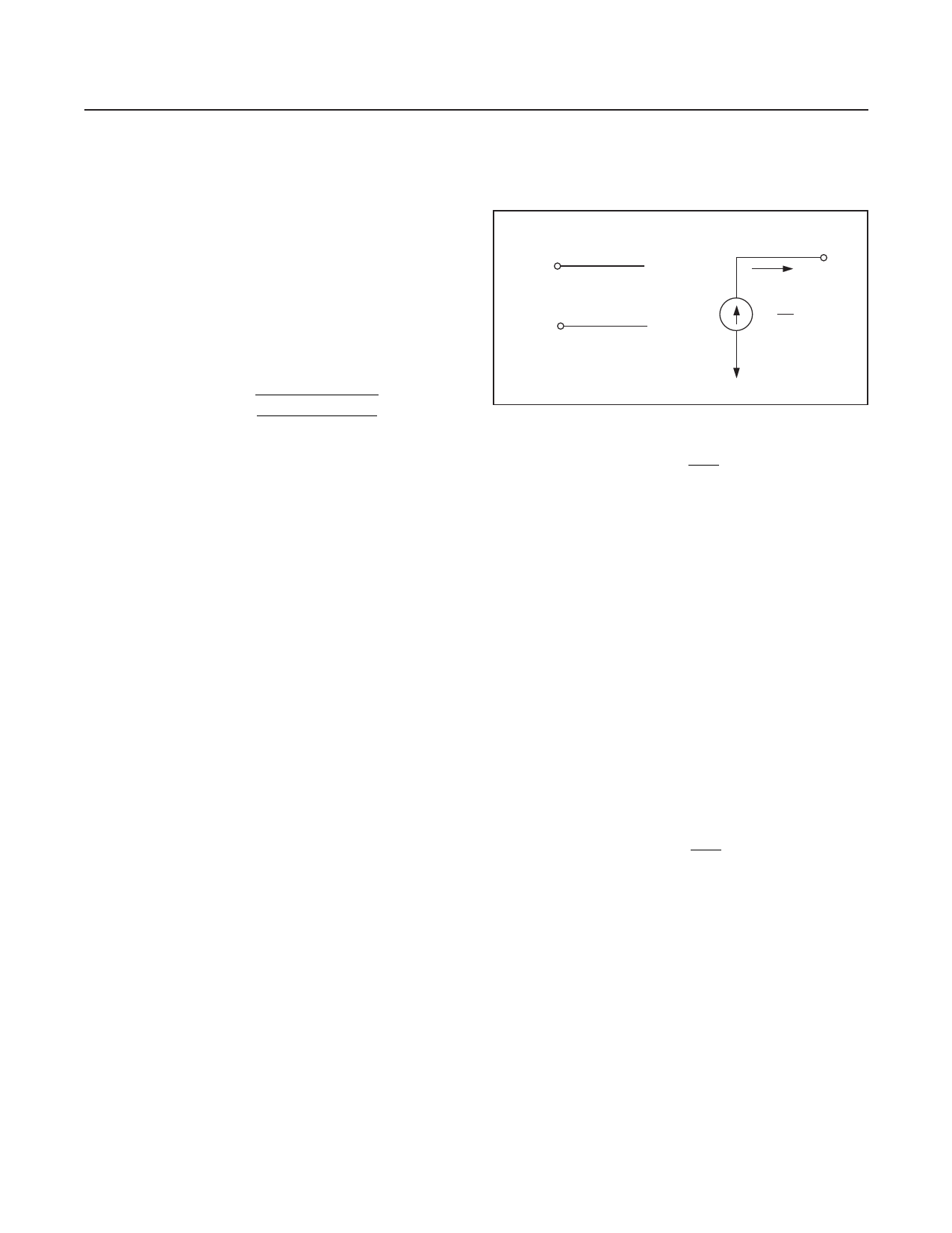
Differential Video Interface Chipset
Applications Information
Differential Interface
The impedances of the differential interface are made
up of the two source resistors on the driver (MAX9546)
shown as RS and the load resistors on the receiver
(MAX9547) shown as RT in the Typical Application
Circuit. These resistors are chosen so their sum match-
es the characteristic impedance (Z0) of the differential
transmission line. For example, a Category 5 cable has
a characteristic impedance of 110Ω, so the sum of the
two RS or RT resistors must be 110Ω to correctly drive
the line. To balance the signals they must be equal, so
RS and RT are 55Ω each.
±15kV ESD Protection
As with all Maxim devices, ESD-protection structures
are incorporated on all pins to protect against electro-
static discharges encountered during handling and
assembly. The driver outputs and receiver inputs have
extra protection against static electricity. Maxim’s engi-
neers developed state-of-the-art structures to protect
these pins against ESD of ±15kV without damage. The
ESD structures withstand high ESD in all states: normal
operation and powered down. After an ESD event, the
MAX9546/MAX9547 keep working without latchup. ESD
protection can be tested in various ways; the driver out-
puts and receiver inputs of this product family are char-
acterized for protection to ±15kV using the Human
Body Model. Other ESD test methodologies include IEC
1000-4-2 Contact Discharge and IEC 1000-4-2 Air-Gap
Discharge (formerly IEC 801-2).
ESD Test Conditions
ESD performance depends on a variety of conditions.
Contact Maxim for a reliability report that documents
test setup, test methodology, and test results.
Human Body Model
Figure 2 shows the Human Body Model, and Figure 3
shows the current waveform it generates when dis-
charged into a low impedance. This model consists of
a 100pF capacitor charged to the ESD voltage of inter-
est, which is then discharged into the test device
through a 1.5kΩ resistor.
RC
1MΩ
RD
1.5kΩ
CHARGE-CURRENT-
LIMIT RESISTOR
DISCHARGE
RESISTANCE
HIGH-
VOLTAGE
DC
SOURCE
Cs
100pF
STORAGE
CAPACITOR
Figure 2. Human Body ESD Test Model
DEVICE
UNDER
TEST
IP 100%
90%
AMPERES
36.8%
10%
0
0 tRL
Ir
PEAK-TO-PEAK RINGING
(NOT DRAWN TO SCALE)
TIME
tDL
CURRENT WAVEFORM
Figure 3. Human Body Current Waveform
_______________________________________________________________________________________ 9
Share Link: 