MCRF450 View Datasheet(PDF) - Microchip Technology
Part Name
Description
Manufacturer
MCRF450 Datasheet PDF : 50 Pages
| |||
MCRF450/451/452/455
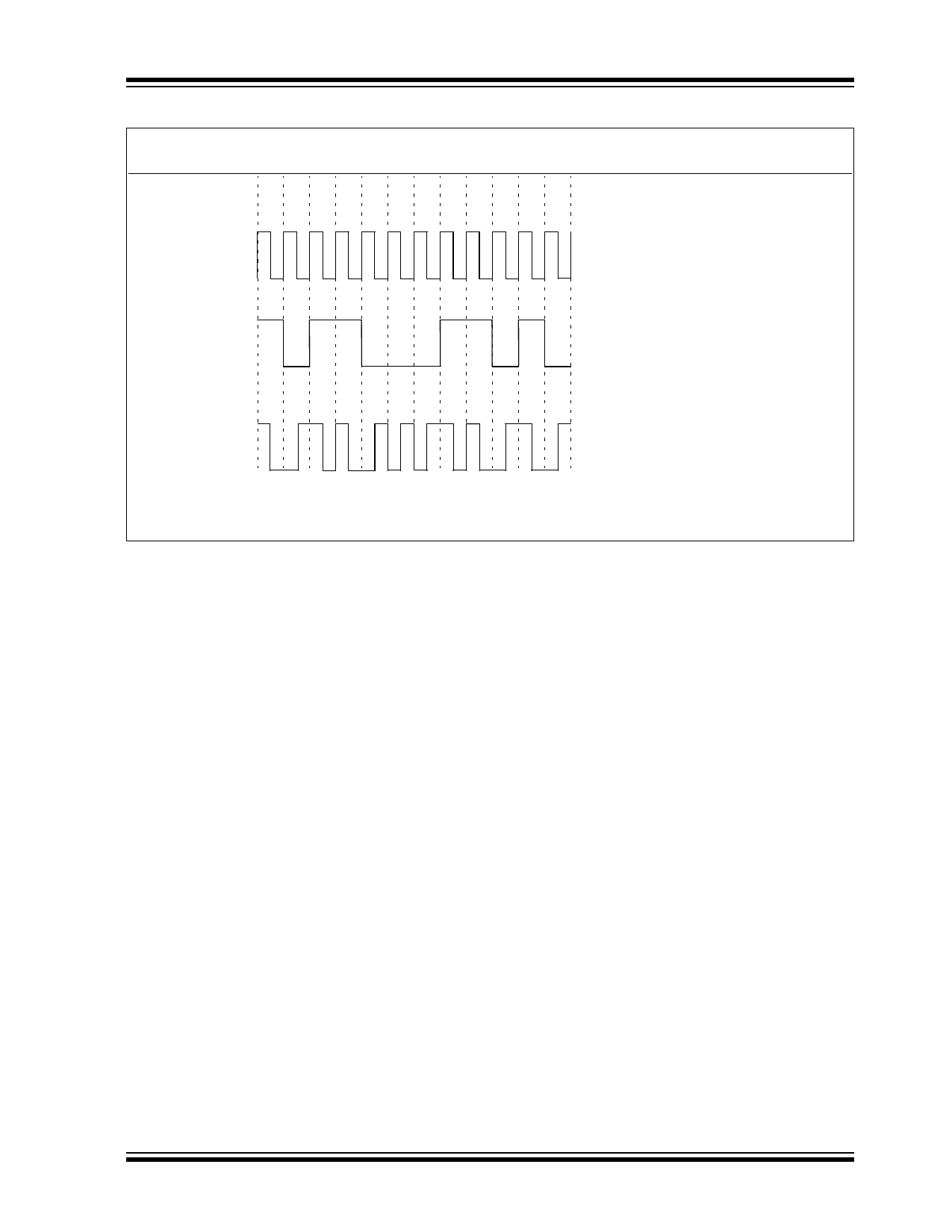
FIGURE 3-2:
SIGNAL
DATA WAVEFORM OF DEVICE
WAVEFORM
DESCRIPTION
Data 1 0 1 1 0 0 0 1 1 0 1 0 Digital Data
CLK
Internal Clock Signal
NRZ - L
(Reference only)
Non Return to Zero - Level
“1” is represented by logic high level.
“0” is represented by logic low level.
BIPHASE - L
(Manchester)
Biphase - Level (Split Phase)
A level change occurs at middle of
every bit clock period.
“1” is represented by a high to low
level change at midclock.
“0” is represented by a low to high
level change at midclock.
2003 Microchip Technology Inc.
DS40232H-page 13
Share Link: 