RJK5014DPP View Datasheet(PDF) - Renesas Electronics
Part Name
Description
Manufacturer
RJK5014DPP Datasheet PDF : 7 Pages
| |||
RJK5014DPP
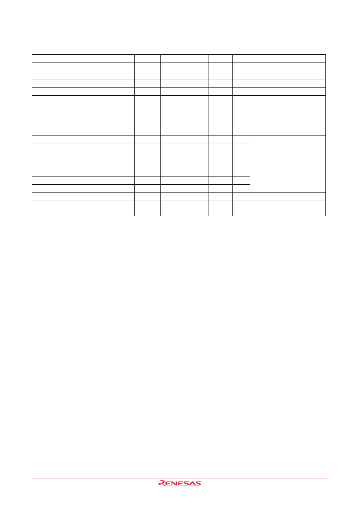
Electrical Characteristics
Item
Symbol Min
Drain to source breakdown voltage
V(BR)DSS
500
Zero gate voltage drain current
IDSS
—
Gate to source leak current
IGSS
—
Gate to source cutoff voltage
VGS(off)
3.0
Static drain to source on state
resistance
RDS(on)
—
Input capacitance
Ciss
—
Output capacitance
Coss
—
Reverse transfer capacitance
Crss
—
Turn-on delay time
td(on)
—
Rise time
tr
—
Turn-off delay time
td(off)
—
Fall time
tf
—
Total gate charge
Qg
—
Gate to source charge
Qgs
—
Gate to drain charge
Qgd
—
Body-drain diode forward voltage
VDF
—
Body-drain diode reverse recovery time
trr
—
Notes: 5. Pulse test
Typ
—
—
—
—
0.325
Max
—
1
±0.1
4.5
0.390
Unit
V
μA
μA
V
Ω
(Ta = 25°C)
Test conditions
ID = 10 mA, VGS = 0
VDS = 500 V, VGS = 0
VGS = ±30 V, VDS = 0
VDS = 10 V, ID = 1 mA
ID = 9.5 A, VGS = 10 V Note5
1800
190
24
36
41
93
39
46
9
20
0.91
320
—
—
—
—
—
—
—
—
—
—
1.55
—
pF VDS = 25 V
pF VGS = 0
pF f = 1 MHz
ns ID = 9.5 A
ns VGS = 10 V
ns RL = 26.3 Ω
ns Rg = 10 Ω
nC VDD = 400 V
nC VGS = 10 V
nC ID = 19 A
V IF = 19 A, VGS = 0 Note5
ns IF = 19 A, VGS = 0
diF/dt = 100 A/μs
REJ03G1530-0200 Rev.2.00 Dec 02, 2009
Page 2 of 6
Share Link: 