SST25LF080A View Datasheet(PDF) - Silicon Storage Technology
Part Name
Description
Manufacturer
SST25LF080A Datasheet PDF : 25 Pages
| |||
8 Mbit SPI Serial Flash
SST25LF080A
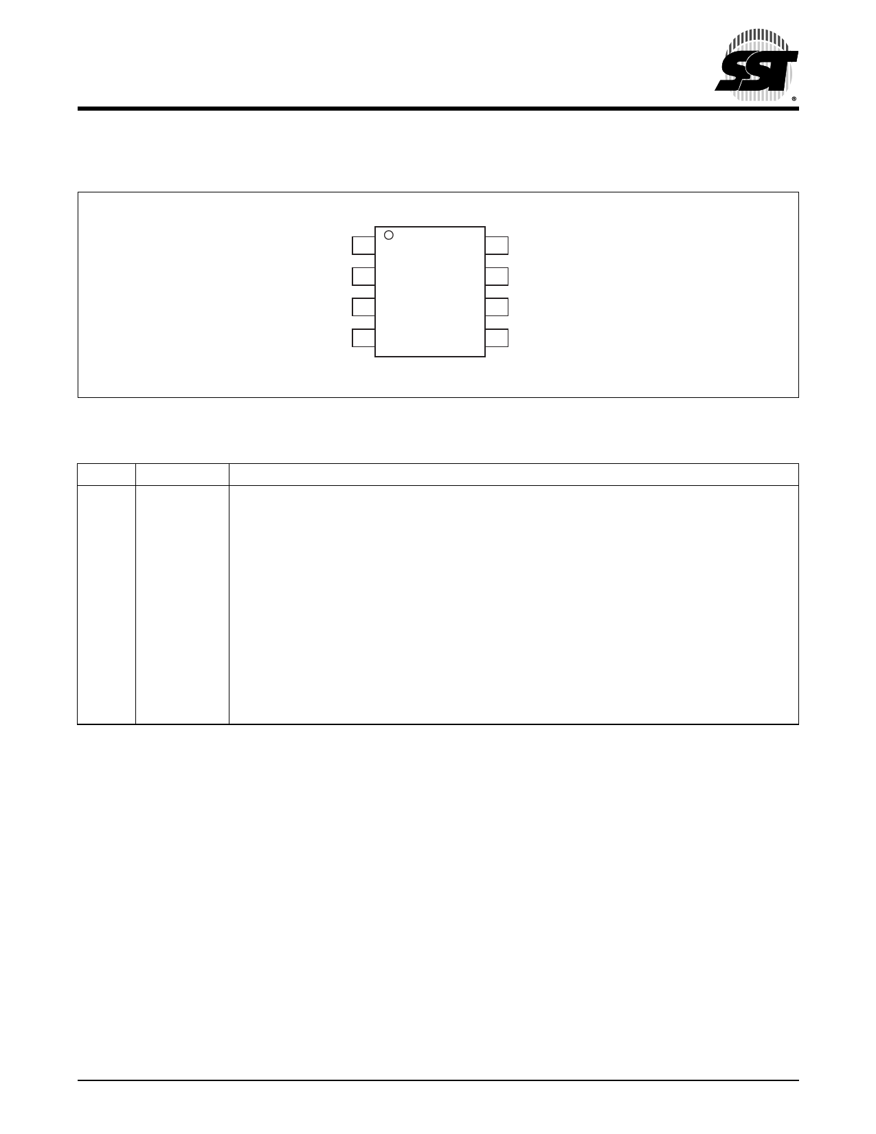
PIN DESCRIPTION
EOL Product Data Sheet
CE#
SO
WP#
VSS
1
8
2
7
Top View
3
6
VDD
HOLD#
SCK
4
5
SI
1248 08-soic P1.0
FIGURE 1: PIN ASSIGNMENTS FOR 8-LEAD SOIC
TABLE 1: PIN DESCRIPTION
Symbol Pin Name
SCK Serial Clock
SI
Serial Data
Input
SO
Serial Data
Output
CE#
Chip Enable
WP#
HOLD#
VDD
VSS
Write Protect
Hold
Power Supply
Ground
Functions
To provide the timing of the serial interface.
Commands, addresses, or input data are latched on the rising edge of the clock input, while output
data is shifted out on the falling edge of the clock input.
To transfer commands, addresses, or data serially into the device.
Inputs are latched on the rising edge of the serial clock.
To transfer data serially out of the device.
Data is shifted out on the falling edge of the serial clock.
The device is enabled by a high to low transition on CE#. CE# must remain low for the duration of
any command sequence.
The Write Protect (WP#) pin is used to enable/disable BPL bit in the status register.
To temporarily stop serial communication with SPI flash memory without resetting the device.
To provide power supply voltage: 3.0-3.6V for SST25LF080A
T1.0 1248
©2006 Silicon Storage Technology, Inc.
3
S71248-06-EOL
1/06
Share Link: 