QT160 View Datasheet(PDF) - Quantum Research Group
Part Name
Description
Manufacturer
QT160 Datasheet PDF : 12 Pages
| |||
1 - OVERVIEW
Option pins allow the selection of several timing features.
QT160/161 is a 6-channel burst mode digital charge-transfer
(QT) sensor designed specifically for touch controls; they
include all hardware and signal processing functions
necessary to provide stable sensing under a wide variety of
conditions. Only a single low cost, non-critical capacitor per
channel is required for operation.
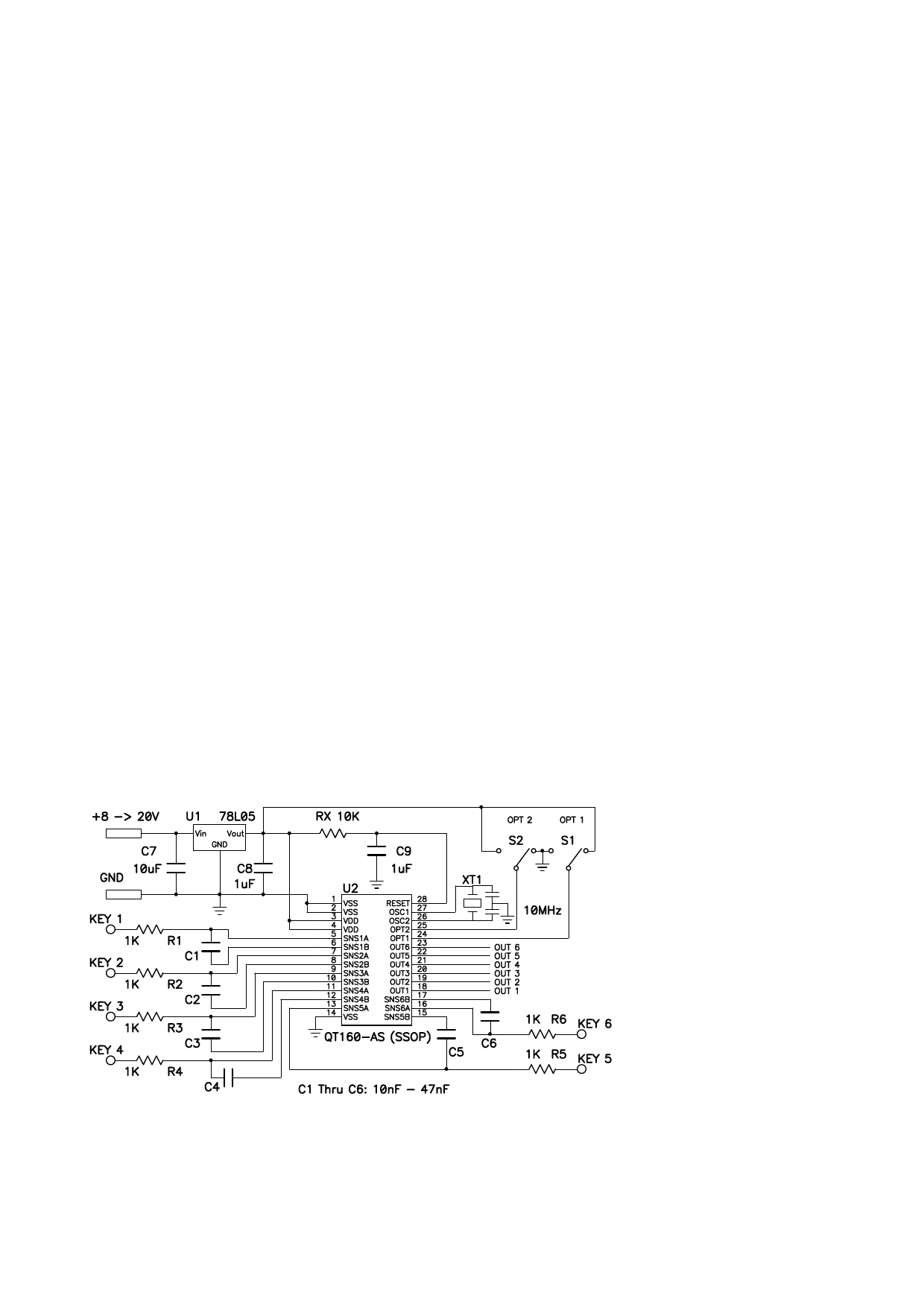
Figure 1-1 shows the basic circuit using the device. See
Tables 7-1 and 7-2 (page 11) for pin listings. The DIP and
SOIC pinouts are not the same and serious damage can
occur if a part is mis-wired).
1.1 BASIC OPERATION
The devices employ bursts of charge-transfer cycles to
acquire signals. Burst mode permits low power operation,
dramatically reduces RF emissions, lowers susceptibility to
RF fields, and yet permits excellent speed. Internally, signals
are digitally processed to reject impulse noise using a
'consensus' filter that requires three consecutive
confirmations of detection. Each channel is measured in
sequence starting with channel 1.
1.2 ELECTRODE DRIVE
The devices have 6 independent channels. The internal ADC
treats Cs on each channel as a floating transfer capacitor; as
a direct result, the sense electrode can be connected to
either SNS1A or SN1B with no performance difference. In
both cases the rule Cs >> Cx must be observed for proper
operation. The polarity of the charge buildup across Cs
during a burst is the same in either case.
It is possible to connect separate Cx and Cx’ loads to
SNS1A and SNS1B simultaneously, although the result is no
different than if the loads were connected together at SNS1A
(or SNS1B). It is important to limit the amount of stray
capacitance on both terminals, especially if the load Cx is
already large, for example by minimizing trace lengths and
widths so as not to exceed the Cx load specification and to
allow for a larger sensing electrode size if so desired.
Unused channels: If a channel is not used, a dummy
nominal 1nF sense capacitor of any type must be connected
to the SNS pins ensure correct operation.
The QT switches and charge measurement hardware
functions are all internal to the device (Figure 1-2). A 14-bit
single-slope switched capacitor ADC includes both the
required QT charge and transfer switches in a configuration
that provides direct ADC conversion. The ADC is designed
to dynamically optimize the QT burst length according to the
rate of charge buildup on Cs, which in turn depends on the
The PCB traces, wiring, and any components associated
with or in contact with SNS1A and SNS1B will become touch
sensitive and should be treated with caution to limit the touch
area to the desired location. Multiple touch electrodes can be
used, for example to create a control button on both sides of
an object, however it is impossible for the sensor to
distinguish between the two touch areas.
values of Cs, Cx, and Vdd. Vdd is used as the charge
reference voltage. Larger values of Cx cause the charge
1.3 KEY DESIGN
transferred into Cs to rise more rapidly, reducing available
resolution; as a minimum resolution is required for proper
1.3.1 KEY GEOMETRY AND SIZE
operation, this can result in dramatically reduced apparent
There is no restriction on the shape of the key electrode; in
gain. Conversely, larger values of Cs reduce the rise of
most cases common sense and a little experimentation can
differential voltage across it, increasing available resolution result in a good electrode design. The devices will operate
by permitting longer QT bursts. The value of Cs can thus be equally well with long, thin keys as with round or square
increased to allow larger values of Cx to be tolerated. The IC ones; even random shapes are acceptable. The electrode
is responsive to both Cx and Cs, and changes in Cs can
can also be a 3-dimensional surface or object. Sensitivity is
result in substantial changes in sensor gain.
related to the amount of surface metallization, touch contact
area, overlying panel material and thickness, and ground
coupling quality of the sensor
Figure 1-1 Recommended Basic Circuit (SSOP Package)
circuit.
If a relatively large touch area is
desired, and if tests show that
the electrode has more
capacitance than the part can
tolerate, the electrode can be
made into a sparse mesh (Figure
1-3) having lower Cx than a solid
plane.
1.3.2 BACKLIGHTING KEYS
Touch pads can be
back-illuminated quite readily
using electrodes with a hole in
the middle (Figure 1-4). The
holes can be as large as 4 cm in
diameter provided that the ring of
metal is at least twice as wide as
the thickness of the overlying
panel, and the panel is greater
than 1/8 as thick as the diameter
of the hole. Thin panels do not
work well with this method they
lQ
2
QT160/161 1.07/0904
Share Link: 