USB1T11A View Datasheet(PDF) - Fairchild Semiconductor
Part Name
Description
Manufacturer
USB1T11A Datasheet PDF : 11 Pages
| |||
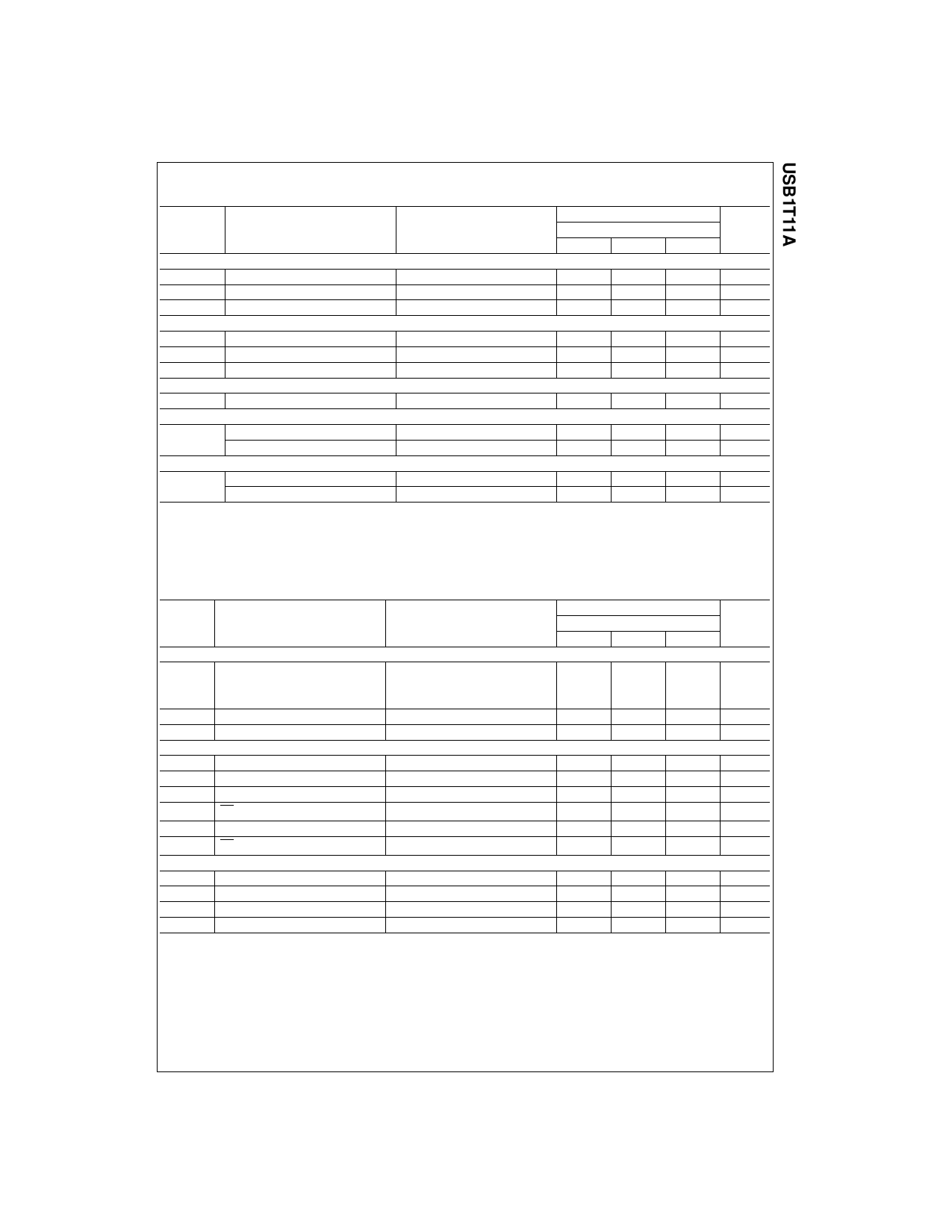
DC Electrical Characteristics (D/D Pins)
Over recommended range of supply voltage and operating free air temperature (unless otherwise noted). VCC 3.0V to 3.6V
Limits
Symbol
Parameter
Test Conditions
Temp 40qC to 85qC
Units
Min
Typ
Max
INPUT LEVELS:
VDI
Differential Input Sensitivity
|(D) – (D)|
0.2
V
VCM
Differential Common Mode Range
Includes VDI Range
0.8
2.5
V
VSE
Single Ended Receiver Threshold
0.8
2.0
V
OUTPUT LEVELS:
VOL
Static Output LOW Voltage
RL of 1.5 k: to 3.6V
0.3
V
VOH
Static Output HIGH Voltage
RL of 15 k: to GND
2.8
3.6
V
VCR
Differential Crossover
1.3
2.0
V
LEAKAGE CURRENT:
IOZ
High Z State Data Line Leakage Current 0V VIN 3.3V
CAPACITANCE:
r5
PA
CIN(Note 6)
Transceiver Capacitance
Capacitance Match
Pin to GND
10
pF
10
%
OUTPUT RESISTANCE:
ZDRV (Note 5) Driver Output Resistance
Resistance Match
Steady State Drive
4
20
:
10
%
Note 5: Excludes external resistor. In order to comply with USB Specification 1.1, external series resistors of 24: r 1% each on D and D are recom-
mended. This specification is guaranteed by design and statistical process distribution.
Note 6: This specification is guaranteed by design and statistical process distribution.
AC Electrical Characteristics (D/D Pins, Full Speed)
Over recommended range of supply voltage and operating free air temperature (unless otherwise noted). VCC 3.0V to 3.6V
CL 50 pF; RL 1.5 k: on D to VCC
Limits
Symbol
Parameter
Test Condition
Temp 40qC to 85qC
Min
Typ
Max
DRIVER CHARACTERISTICS:
10% and 90%
tR
tF
tRFM
VCRS
Rise Time
Fall Time
Rise/Fall Time Matching
Output Signal Crossover Voltage
DRIVER TIMINGS:
Figure 1
Figure 1
(tr/tf)
4
20
4
20
90
110
1.3
2.0
tPLH
Driver Propagation Delay
Figure 2
18
tPLH
(VPO, VMO/FSEO to D/D)
Figure 2
18
tPHZ
Driver Disable Delay
Figure 4
13
tPLZ
(OE to D/D)
Figure 4
13
tPZH
Driver Enable Delay
Figure 4
17
tPZL
(OE to D/D)
Figure 4
17
RECEIVER TIMINGS:
tPLH
Receiver Propagation Delay
Figure 3
16
tPHL
(D, D to RCV)
Figure 3
19
tPLH
Single-ended Receiver Delay
Figure 3
8
tPHL
(D, D to VP, VM)
Figure 3
8
Units
ns
%
V
ns
ns
ns
ns
ns
ns
ns
ns
ns
ns
5
www.fairchildsemi.com
Share Link: 