VN5016AJTR-E View Datasheet(PDF) - STMicroelectronics
Part Name
Description
Manufacturer
VN5016AJTR-E
STMicroelectronics

VN5016AJTR-E Datasheet PDF : 32 Pages
| |||
VN5016AJ-E
Block diagram and pin description
1
Block diagram and pin description
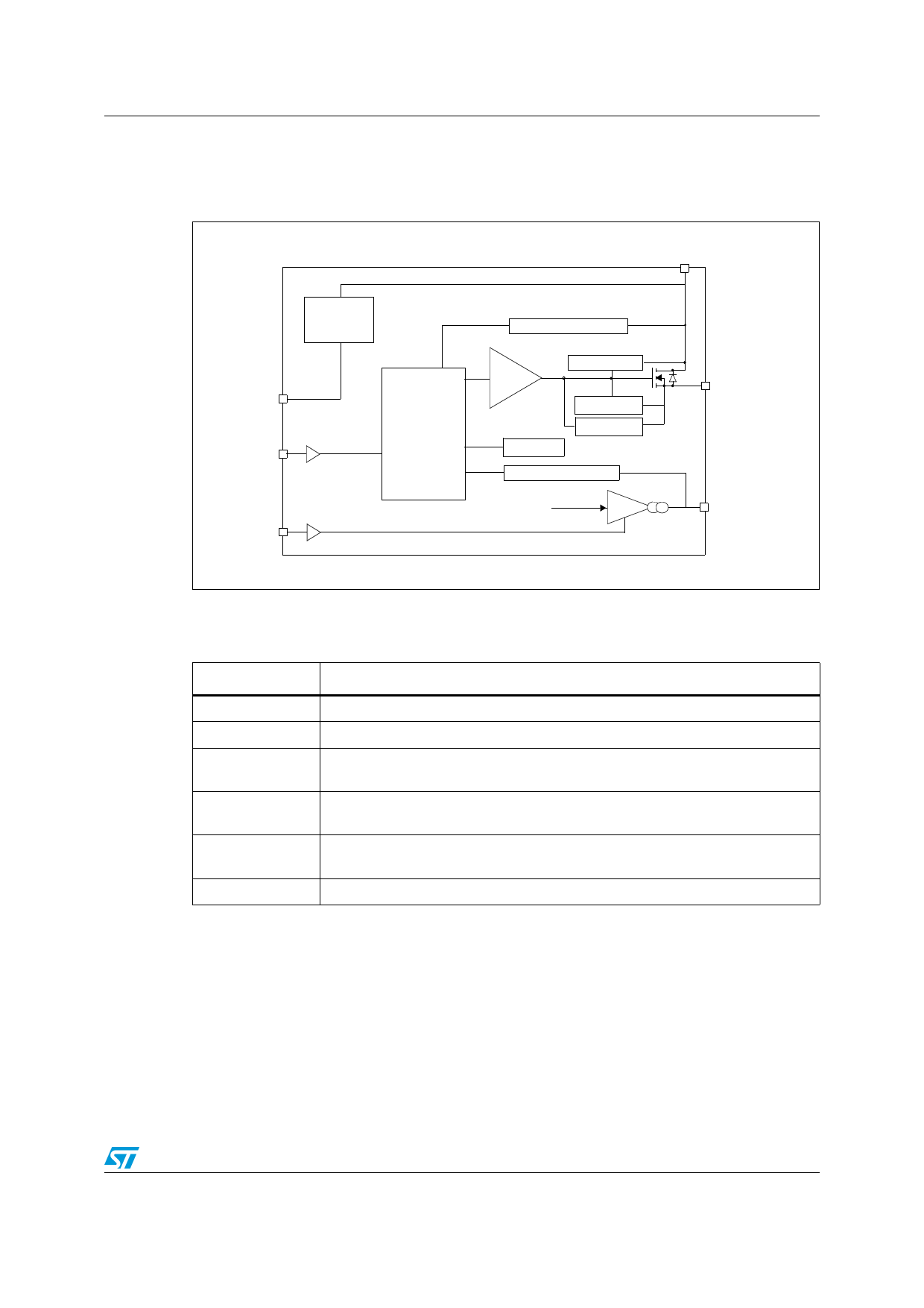
Figure 1. Block diagram
VCC
GND
INPUT
CS_DIS
VCC
CLAMP
LOGIC
UNDERVOLTAGE
DRIVER
PwCLAMP
PwrLIM
ILIM
VDSLIM
OVERTEMP.
IOUT
K
OUTPUT
CURRENT
SENSE
Table 2. Pin function
Name
Function
VCC
OUTPUT
Battery connection.
Power output.
GND
INPUT
CURRENT
SENSE
CS_DIS
Ground connection. Must be reverse battery protected by an external
diode/resistor network.
Voltage controlled input pin with hysteresis, CMOS compatible. Controls output
switch state.
Analog current sense pin, delivers a current proportional to the load current.
Active high CMOS compatible pin, to disable the current sense pin.
5/32
Share Link: