WED3EG7232S403JD3 View Datasheet(PDF) - White Electronic Designs Corporation
Part Name
Description
Manufacturer
WED3EG7232S403JD3 Datasheet PDF : 12 Pages
| |||
WED3EG7232S-JD3
PRELIMINARY
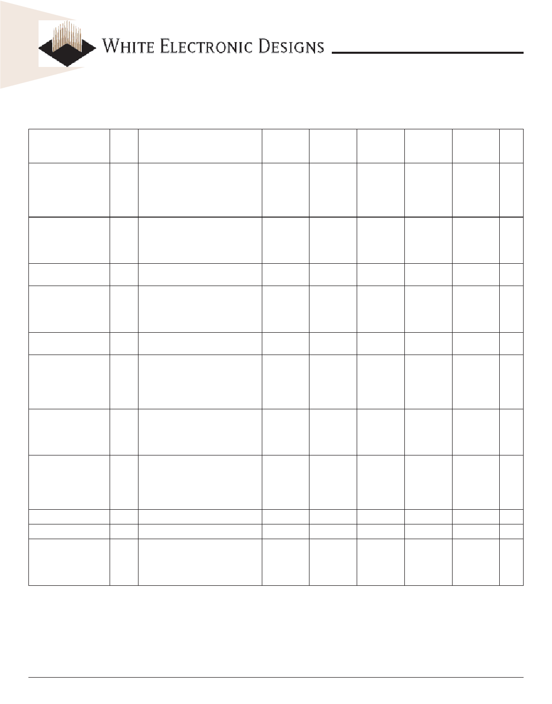
IDD SPECIFICATIONS AND TEST CONDITIONS
DDR400: VCC = VCCQ = +2.6V ± 0.1V; DDR333, 266, 200: VCC = VCCQ = 2.5V ± 0.2V
Includes DDR SDRAM component only
Parameter
Symbol Conditions
Operating Current
IDD0 One device bank; Active - Precharge;
tRC=tRC (MIN); tCK=tCK (MIN); DQ,DM
and DQS inputs changing once per
clock cycle; Address and control
inputs changing once every two
cycles.
Operating Current
IDD1 One device bank; Active-Read-
Precharge Burst = 2; tRC=tRC (MIN);
tCK=tCK (MIN); lOUT = 0mA; Address
and control inputs changing once per
clock cycle.
Precharge Power-
IDD2P All device banks idle; Power-down
Down Standby Current
mode; tCK=tCK (MIN); CKE=(low)
Idle Standby Current
IDD2F CS# = High; All device banks idle;
tCK=tCK (MIN); CKE = high; Address
and other control inputs changing
once per clock cycle. VIN = VREF for
DQ, DQS and DM.
Active Power-Down
Standby Current
IDD3P One device bank active; Power-
Down mode; tCK (MIN); CKE=(low)
Active Standby Current IDD3N CS# = High; CKE = High; One device
bank; Active-Precharge; tRC=tRAS
(MAX); tCK=tCK (MIN); DQ, DM and
DQS inputs changing twice per clock
cycle; Address and other control
inputs changing once per clock cycle.
Operating Current
IDD4R Burst = 2; Reads; Continuous burst;
One device bank active; Address
and control inputs changing once
per clock cycle; TCK= TCK (MIN); lOUT
= 0mA.
Operating Current
IDD4W Burst = 2; Writes; Continuous burst;
One device bank active; Address
and control inputs changing once per
clock cycle; tCK=tCK (MIN); DQ,DM
and DQS inputs changing once per
clock cycle.
Auto Refresh Current IDD5 tRC = tRC (MIN)
Self Refresh Current
IDD6 CKE ≤ 0.2V
Operating Current
IDD7A Four bank interleaving Reads (BL=4)
with auto precharge with tRC=tRC
(MIN); tCK=tCK (MIN); Address and
control inputs change only during
Active Read or Write commands.
DDR400@
CL=3
Max
1215
1530
36
540
360
630
1800
1755
2340
36
4230
DDR333@
CL=2.5
Max
1125
1530
36
450
270
540
1575
1575
2295
36
3690
DDR266@
CL=2
Max
1125
1530
36
450
270
540
1575
1575
2295
36
3690
DDR266@
CL=2.5
Max
1125
1530
36
450
270
540
1575
1575
2295
36
3690
DDR200@
CL=2
Max Units
1125
mA
1530
mA
36
rnA
450
mA
270
mA
540
mA
1575
mA
1575
rnA
2295
mA
36
mA
3690
mA
June 2006
Rev. 6
5
White Electronic Designs Corporation • (602) 437-1520 • www.wedc.com
Share Link: 