LPC1768 View Datasheet(PDF) - NXP Semiconductors.
Part Name
Description
Manufacturer
LPC1768 Datasheet PDF : 79 Pages
| |||
NXP Semiconductors
LPC1769/68/67/66/65/64/63
32-bit ARM Cortex-M3 microcontroller
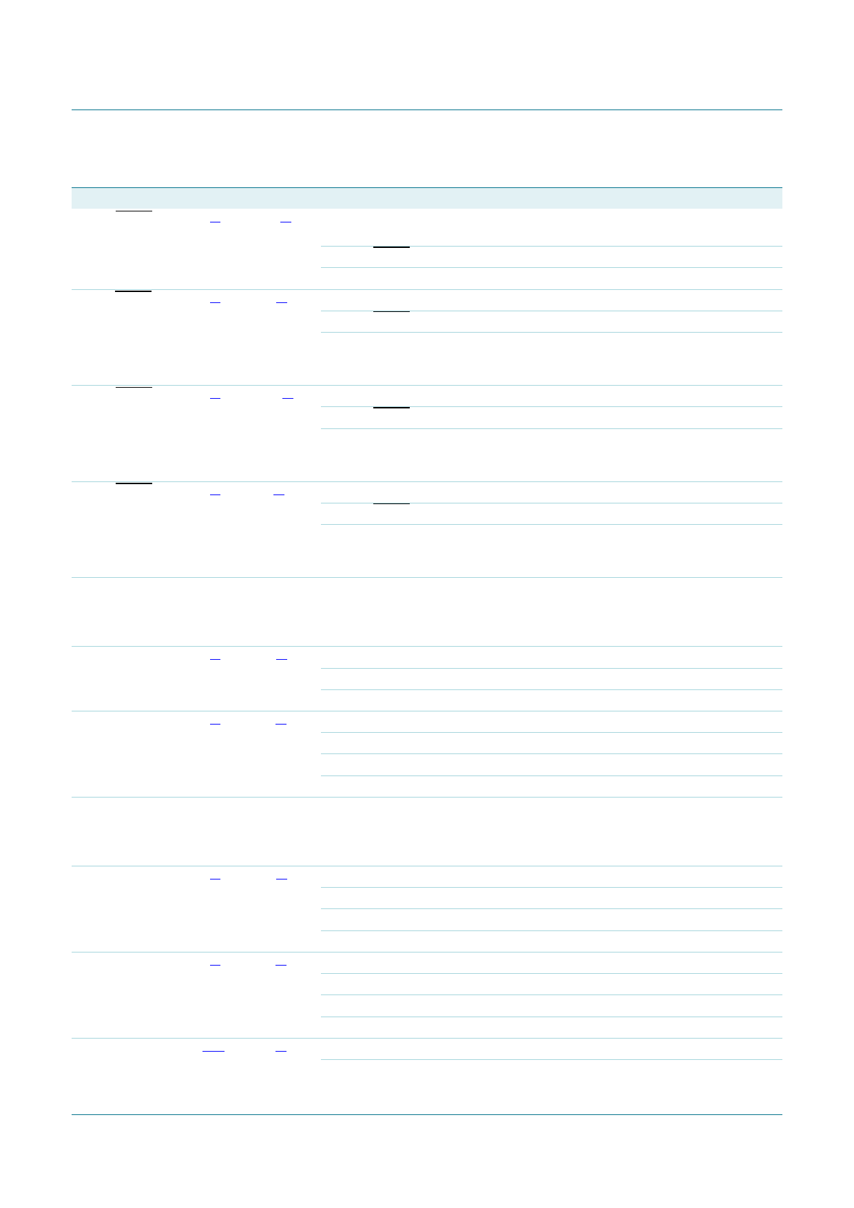
Table 4. Pin description …continued
Symbol
Pin
Ball
P2[10]/EINT0/NMI 53[6]
J10[6]
P2[11]/EINT1/
I2STX_CLK
52[6]
H8[6]
P2[12]/EINT2/
I2STX_WS
51[6]
K10[6]
P2[13]/EINT3/
I2STX_SDA
50[6]
J9[6]
P3[0] to P3[31]
P3[25]/MAT0[0]/
PWM1[2]
27[1]
H3[1]
P3[26]/STCLK/
26[1]
MAT0[1]/PWM1[3]
K1[1]
P4[0] to P4[31]
P4[28]/RX_MCLK/ 82[1]
MAT2[0]/TXD3
C7[1]
P4[29]/TX_MCLK/ 85[1]
MAT2[1]/RXD3
E6[1]
TDO/SWO
1[1][7]
A1[1]
Type
I/O
I
I
I/O
I
I/O
I/O
I
I/O
I/O
I
I/O
I/O
I/O
O
O
I/O
I
O
O
I/O
I/O
I
O
O
I/O
I
O
I
O
O
Description
P2[10] — General purpose digital input/output pin. A LOW level on this
pin during reset starts the ISP command handler.
EINT0 — External interrupt 0 input.
NMI — Non-maskable interrupt input.
P2[11] — General purpose digital input/output pin.
EINT1 — External interrupt 1 input.
I2STX_CLK — Transmit Clock. It is driven by the master and received
by the slave. Corresponds to the signal SCK in the I2S-bus
specification. (LPC1769/68/67/66/65/63 only).
P2[12] — General purpose digital input/output pin.
EINT2 — External interrupt 2 input.
I2STX_WS — Transmit Word Select. It is driven by the master and
received by the slave. Corresponds to the signal WS in the I2S-bus
specification. (LPC1769/68/67/66/65/63 only).
P2[13] — General purpose digital input/output pin.
EINT3 — External interrupt 3 input.
I2STX_SDA — Transmit data. It is driven by the transmitter and read
by the receiver. Corresponds to the signal SD in the I2S-bus
specification. (LPC1769/68/67/66/65/63 only).
Port 3: Port 3 is a 32-bit I/O port with individual direction controls for
each bit. The operation of port 3 pins depends upon the pin function
selected via the pin connect block. Pins 0 through 24, and 27 through
31 of this port are not available.
P3[25] — General purpose digital input/output pin.
MAT0[0] — Match output for Timer 0, channel 0.
PWM1[2] — Pulse Width Modulator 1, output 2.
P3[26] — General purpose digital input/output pin.
STCLK — System tick timer clock input.
MAT0[1] — Match output for Timer 0, channel 1.
PWM1[3] — Pulse Width Modulator 1, output 3.
Port 4: Port 4 is a 32-bit I/O port with individual direction controls for
each bit. The operation of port 4 pins depends upon the pin function
selected via the pin connect block. Pins 0 through 27, 30, and 31 of this
port are not available.
P4[28] — General purpose digital input/output pin.
RX_MCLK — I2S receive master clock. (LPC1769/68/67/66/65 only).
MAT2[0] — Match output for Timer 2, channel 0.
TXD3 — Transmitter output for UART3.
P4[29] — General purpose digital input/output pin.
TX_MCLK — I2S transmit master clock. (LPC1769/68/67/66/65 only).
MAT2[1] — Match output for Timer 2, channel 1.
RXD3 — Receiver input for UART3.
TDO — Test Data out for JTAG interface.
SWO — Serial wire trace output.
LPC1769_68_67_66_65_64_63
Product data sheet
All information provided in this document is subject to legal disclaimers.
Rev. 7 — 5 April 2011
© NXP B.V. 2011. All rights reserved.
15 of 79
Share Link: 