DSP56302 View Datasheet(PDF) - Motorola => Freescale
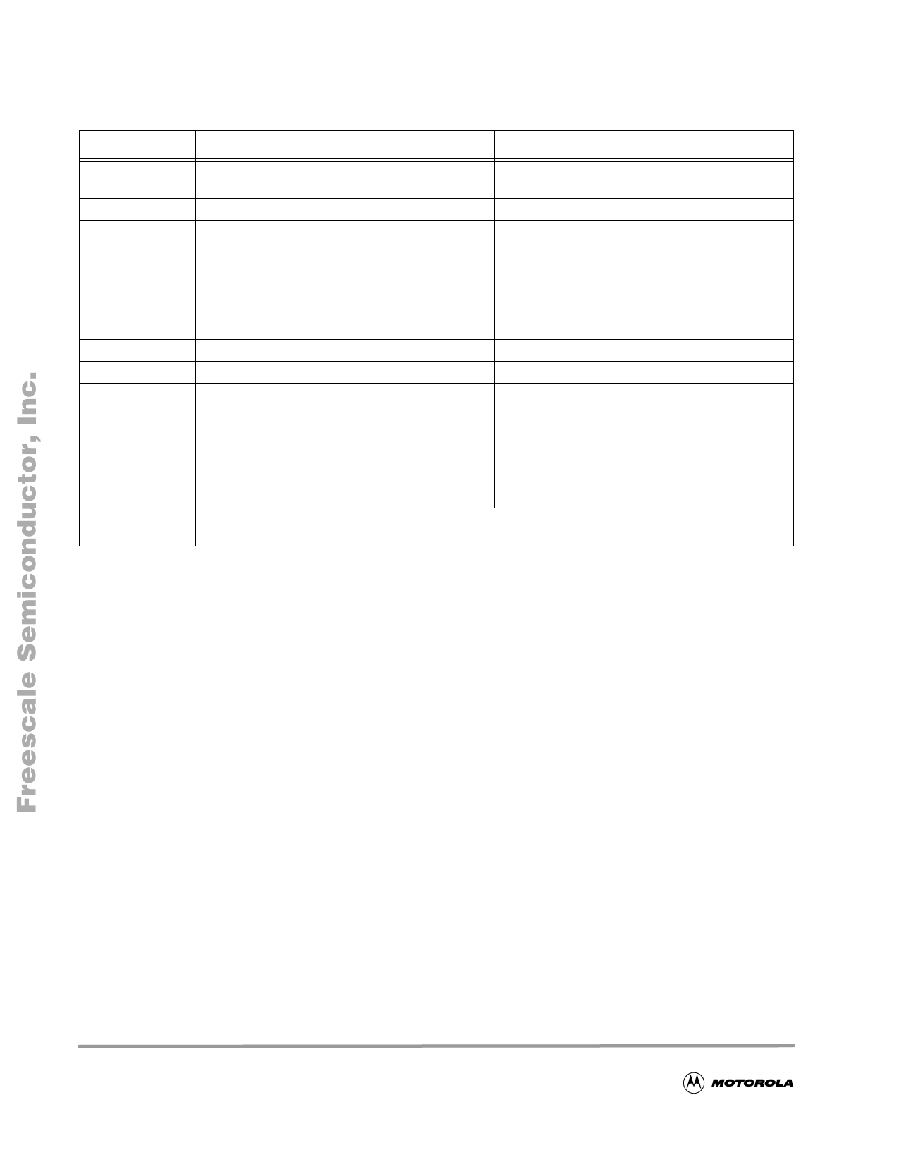
Part Name
Description
Manufacturer
DSP56302 Datasheet PDF : 6 Pages
| |||
Freescale Semiconductor, Inc.
Feature
Operating
frequency
Technology
Input power
I/O pins
Package
PLL input
capacitor
(CPCAP)
Operating
modes
Other
functionality
Table 1. Functional Comparison of DSP56302 and DSP56309
DSP56302
≤ 66 MHz down to 0 Hz
DSP56309
≤ 100 MHz down to 0 Hz
0.5 micron
VCC = 3.0-3.6 V combined core and I/O power
and ground
5 V tolerant (exceptions: see data sheet)
144-pin TQFP
Uses the following rules:
For MF ≤ 4:
CPCAP = [(500 × MF) – 150] pF
For MF > 4:
CPCAP = (690 × MF) pF
Sub 0.4 micron
Split power:
Core VCC (3.0–3.6 V currently)
I/O VCC (3.0–3.6 V currently)
A pinout change is required to support the split
power configuration. See Section 3 for more
information and a description of the pinout
change for the 144-pin TQFP package.
Tolerant up to 3.6 V
144-pin TQFP or 196-pin PBGA
Uses the following rules:
For MF ≤ 4:
CPCAP = [(680 × MF) – 120] pF
For MF > 4:
CPCAP = (1100 × MF) pF
See Table 3 for details.
All memory, control functions, and peripherals are identical. Refer to the DSP56309 Technical
Data Sheet (order by DSP56309/D) for a detailed description of these features.
3 Input Power Changes
One method to increase the operating frequency of an integrated circuit is to “shrink” the die (that is,
reduce the die dimensions, both linearly and vertically). Reducing the die size can yield additional benefits,
such as a reduction of power consumption, but can also result in other functional changes. The DSP56309
is a “shrink” of the DSP56302. This die size reduction enables the DSP56309 to achieve higher operating
frequencies. Decreasing the die size, however, requires a reduction of the thickness of the oxide dielectrics,
which also reduces the maximum allowable voltages across some oxides within the die. To support future
“shrinks” of the DSP56309 while maximizing system level compatibility, Motorola has elected to separate
the power supply networks on the die. This split allows the I/O pins to operate over a voltage range which
is different from that used by the core digital logic. Although the initial release of this product specifies the
same voltage ranges for the I/O pins and the core logic, future versions of the DSP56309 or its derivatives
are likely to have reduced core logic VCC requirements (for example, 2.5 V and lower voltages) while the
I/O levels use a higher level (for example, 3.3 V). This allows Motorola to continue aggressively to
“shrink” the device, while preserving the ability to maintain system level compatibility.
The split-power design requires a modification in the chip pinout. A top view of the DSP56309 TQFP
package is shown in Figure 1. Table 2 lists the pin differences between the DSP56302 and the DSP56309.
Note:
The power input for the core logic is designated VCCQ for the DSP56302. For the DSP56309, the
independent core logic input voltage is designated VCCQL, while the independent I/O input voltage
is designated VCCQH. VCCQL should be connected to the core input power supply. VCCQH and all
other input power (VCCA, VCCC, VCCD, VCCH, VCCP, and VCCS) should be connected to the
external input power supply.
2
DSP56302 and DSP56309 Functional Differences
For More Information On This Product,
Go to: www.freescale.com
Share Link: 