ES6028 View Datasheet(PDF) - Unspecified
Part Name
Description
Manufacturer
ES6028 Datasheet PDF : 10 Pages
| |||
ES6028 PRODUCT BRIEF
ES6028 PIN DESCRIPTION
ES6028 PIN DESCRIPTION
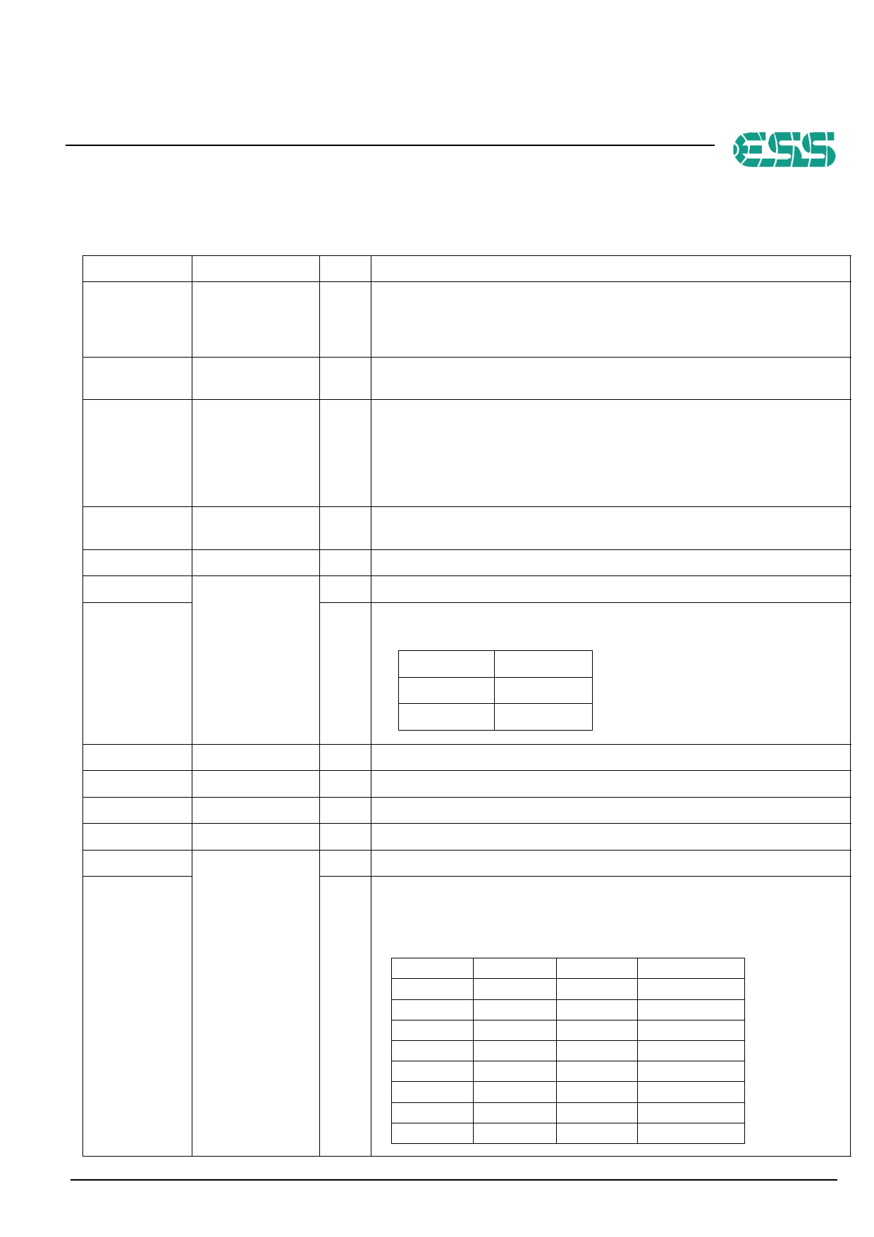
Table 1 lists the pin descriptions for the ES6028.
Table 1 ES6028 Pin Description
Name
Pin Numbers
I/O Definition
VEE
1,18, 27, 59, 68, 75,
92, 99, 104, 130,
148, 157, 159, 164,
183, 193, 201
P I/O power supply.
LA[21:0]
2-7, 10-16, 19-23,
204-207
O RISC port address bus.
VSS
8, 17, 26, 34, 43,
60, 67, 76, 84, 91,
98, 103, 120, 129,
138, 147, 156, 163,
171, 177, 184, 192,
200, 208
G Ground.
VCC
9, 35, 44, 83, 121,
139, 172
P Core power supply.
RESET#
24
I Reset input, active-low.
TDMDX
O TDM transmit data output.
I LCS3 ROM Boot Data Width Select. Strapped to VCC or ground via 4.7-kΩ
resistor; read only during reset.
RSEL
25
RSEL
0
1
Selection
16-bit ROM
8-bit ROM
TDMDR
TDMCLK
TDMFS
TDMTSC#
TWS
SEL_PLL2
28
I TDM receive data input.
29
I TDM clock input.
30
I TDM frame sync input.
31
O TDM output enable.
O Audio transmit frame sync output.
I System and DSCK output clock frequency selection is made at the rising edge of
RESET#. The matrix below lists the available clock frequencies and their
respective PLL bit settings. Strapped to VCC or ground via 4.7-kΩ resistor; read
only during reset.
SEL_PLL2 SEL_PLL1 SEL_PLL0 Clock Type
0
0
0
DCLK x 4.25
32
0
0
1
Reserved
0
1
0
Bypass mode
0
1
1
DCLK x 3.75
1
0
0
DCLK x 4.5
1
0
1
Reserved
1
1
0
DCLK x 3.5
1
1
1
DCLK x 4
ESS Technology, Inc.
SAM0462-031704
3
Share Link: 