71215S10 View Datasheet(PDF) - Integrated Device Technology
Part Name
Description
Manufacturer
71215S10
Integrated Device Technology

71215S10 Datasheet PDF : 14 Pages
| |||
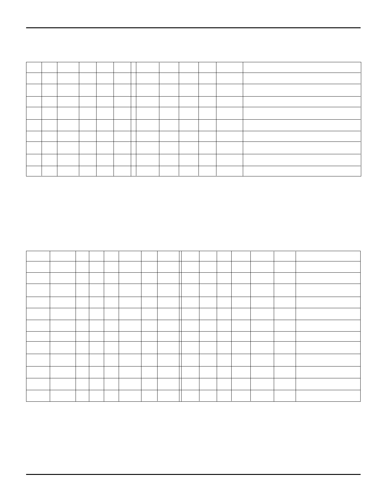
IDT71215
BiCMOS 16Kx15 CACHE-TAG RAM
TRUTH TABLES (CONT.)
COMMERCIAL TEMPERATURE RANGE
MATCH FUNCTION(1, 2, 3)
CS1 CS2 SFUNC OET WET WES
TAG VLD(4) DTY(4) WT(4) MATCH
OPERATION
HX
X
X
XX
Hi-Z –
–
– Hi-Z
Deselected
XL
X
X
XX
Hi-Z –
–
– Hi-Z
Deselected
LH
X
X
XX
–
–
–
–
DOUT
Selected
LH
X
L
HX
DOUT
–
–
–
L
Read Tag I/O
LH
X
H
LX
DIN
–
–
–
L
Write Tag I/O
LH
X
X
XL
–
DIN
DIN DIN
L
Write Status Bits
LH
L
H
HH
TAGIN L
–
–
L
Invalid Data - Dedicated Status Bits
LH
L
H
HH
TAGIN H
–
–
M
Match - Dedicated Status Bits
LH
H
H
HH
TAGIN X
–
–
M
Match - Generic Status Bits
NOTES:
1. "H" = VIH, "L" = VIL, "X" = don't care, "–" = unrelated.
2. M = HIGH if TAGIN equals the memory contents at that address; M = LOW if TAGIN does not equal the memory contents at that address.
3. PWRDN and RESET are HIGH for this table. W/R, BRDYH, , BRDYOE , BRDYIN OES, and CLK are "X".
4. This column represents the stored memory cell data for the given Status bit at the selected address.
3075 tbl 04
BRDY FUNCTION(1, 2, 3, 5)
BRDYOE BRDYIN(6) OET WET WES BRDYH W/R SFUNC VLD(4) DTY(4) WT(4) TAG MATCH BRDY
OPERATION
H
X
X XX
X
XX
X–X–
–
Hi-Z
BRDY Disabled
L
L
X XX
X
XX
X–X–
X
L
Ext BRDY Input (7)
L
H
L XX
X
XX
X
–
X DOUT
L
H
Read TAG
L
H
X LX
X
XX
X
–
X DIN
L
H
Write TAG
L
H
XXL
X
XX
DIN DIN DIN –
L
H
Write Status
L
H
X XX
H
XX
X–X–
X
H
Force BRDY HIGH
L
H
X XX
X
XL
L–X–
L
H
Invalid TAG
L
H
X XX
X
HL
X–H–
X
H
Write Through
L
H
H HH
L
XL
H
–
L TAGIN M
M
Compare
L
H
H HH
L
LL
H – X TAGIN M
M
Compare
L
H
H HH
L
XL
H – X TAGIN M
M
Compare
L
H
H HH
L
XH
X – X TAGIN M
M
Compare
NOTES:
3075 tbl 05
1. "H" = VIH, "L" = VIL, "X" = don't care, "–" = unrelated.
2. M = HIGH if TAGIN equals the memory contents at that address; M = LOW if TAGIN does not equal the memory contents at that address.
3. PWRDN and RESET are HIGH for this table. CLK and OES are "X".
4. This column represents the stored memory cell data for the given Status bit at the selected address.
5. CS1 is LOW, CS2 is HIGH for this table.
6. BRDYIN is a synchronous input; thus the inputs noted in the table must be applied during a rising CLK edge.
7. BRDYIN will be a factor in determining the BRDY output in all cases except when BRDYH is HIGH and there is a valid MATCH. In that case, BRDY will
be LOW(Valid).
14.3
5
Share Link: