71215S10 View Datasheet(PDF) - Integrated Device Technology
Part Name
Description
Manufacturer
71215S10
Integrated Device Technology

71215S10 Datasheet PDF : 14 Pages
| |||
IDT71215
BiCMOS 16Kx15 CACHE-TAG RAM
COMMERCIAL TEMPERATURE RANGE
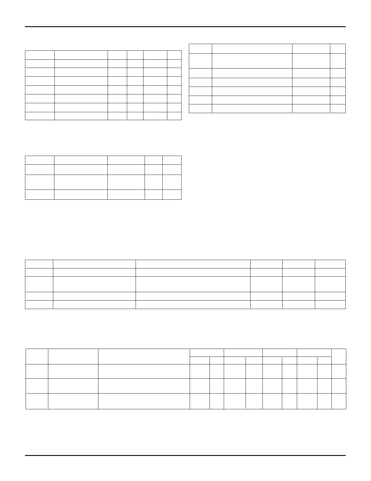
RECOMMENDED DC
OPERATING CONDITIONS
Symbol
Parameter
Min. Typ. Max. Unit
VCC
VCCQ
Supply Voltage
5V Output Buffers
4.75 5.0
4.75 5.0
5.25 V
5.25 V
VCCQ 3.3V Output Buffers 3.0 3.3 3.6 V
VSS
Supply Ground
0
0
0V
VIH
Input High Voltage 2.2 3.0 VCC+0.3 V
VIHQ
I/O High Voltage
2.2 3.0 VCCQ+0.3 V
VIL
Input Low Voltage –0.5(1) —
0.8 V
NOTE:
3075 tbl 06
1. VIL (min.) = –1.5V for pulse width of less than 10ns, once per cycle.
CAPACITANCE
(TA = +25°C, f = 1.0 MHz)
Symbol
Parameter(1)
Condition Max. Unit
CIN
CTAG
COUT
Input Capacitance
VIN = 0V
5
pF
TAG Input/Output
Capacitance
VI/O = 0V
7
pF
Output Capacitance VOUT = 0V
7
pF
NOTE:
3075 tbl 07
1. This parameter is determined by device characterization but is not produc-
tion tested.
ABSOLUTE MAXIMUM RATINGS(1)
Symbol
Rating
VTERM Terminal Voltage with Respect
to GND
TA
Operating Temperature
TBIAS Temperature Under Bias
TSTG Storage Temperature
PT
Power Dissipation
IOUT DC Output Current
Value
Unit
–0.5 to +7.0(2) V
–0 to +70 °C
–65 to +135 °C
–65 to +150 °C
1.7
W
20
mA
NOTES:
3075 tbl 08
1. Stresses greater than those listed under ABSOLUTE MAXIMUM RAT-
INGS may cause permanent damage to the device. This is a stress rating
only and functional operation of the device at these or any other conditions
above those indicated in the operational sections of this specification is not
implied. Exposure to absolute maximum rating conditions for extended
periods may affect reliabilty.
2. VIN should not exceed Vcc+0.5V. All pins should not exceed 7.0V.
VCCQ should never exceed VCC, and VCC should never exceed
VCCQ + 4.0V.
DC ELECTRICAL CHARACTERISTICS OVER THE OPERATING
TEMPERATURE AND SUPPLY VOLTAGE RANGE
(VCC = 5.0V ± 5%, VCCQ = 5.0V ± 5% OR 3.3V ± 0.3V)
Symbol
|ILI|
|ILO|
Parameter
Input Leakage Current
Output Leakage Current
VOL
Output Low Voltage
VOH Output High Voltage
Test Condition
VCC = Max., VIN = 0V to VCC
CS1 ≥ VIH, CS2 ≤ VIL, OE ≥ VIH, VCC = Max.
VOUT = 0V to VCCQ, VCCQ = Max.
IOL = 4mA, VCC = Min.
IOH = –4mA, VCC = Min.
Min.
—
—
—
2.4
Max.
5
5
0.4
—
Unit
µA
µA
V
V
3075 tbl 09
DC ELECTRICAL CHARACTERISTICS OVER THE OPERATING
TEMPERATURE AND SUPPLY VOLTAGE RANGE(1, 2) (VCC = 5.0V ± 5%)
Symbol Parameter
Test Condition
71215S8
Com'l. Mil.
ICC Operating Power PWRDN ≥ VIH
330 —
Supply Current
Outputs Open, VCC = Max., f = fMAX(3)
ISB Standby Power
Supply Current
PWRDN ≤ VIL, VIN ≥ VIH or ≤ VIL
VCC = Max., f = fMAX(3)
30 —
ISB1 Full Standby Power PWRDN ≤ VIL, VIN ≥ VHC or ≤ VLC(4)
Supply Current
VCC = Max., f = 0(3)
25 —
71215S9
Com'l. Mil.
300 —
30
—
25
—
71215S10
Com'l. Mil.
290 —
30 —
25 —
71215S12
Com'l. Mil.
280 —
30 —
25 —
Unit
mA
mA
mA
NOTES:
1. All values are maximum guaranteed values.
2. CS1 ≤ VIL, CS2 ≥ VIH.
3. fMAX =1/tCYC (all address inputs are cycling at fMAX). f = 0 means no address input lines are changing.
4. VHC = VCC - 0.2V, VLC = 0.2V
3075 tbl 10
14.3
6
Share Link: