MAC7100 View Datasheet(PDF) - Motorola => Freescale
Part Name
Description
Manufacturer
MAC7100 Datasheet PDF : 48 Pages
| |||
Freescale Semiconductor, Inc.
Electrical Characteristics
3.8.3 PLL Characteristics
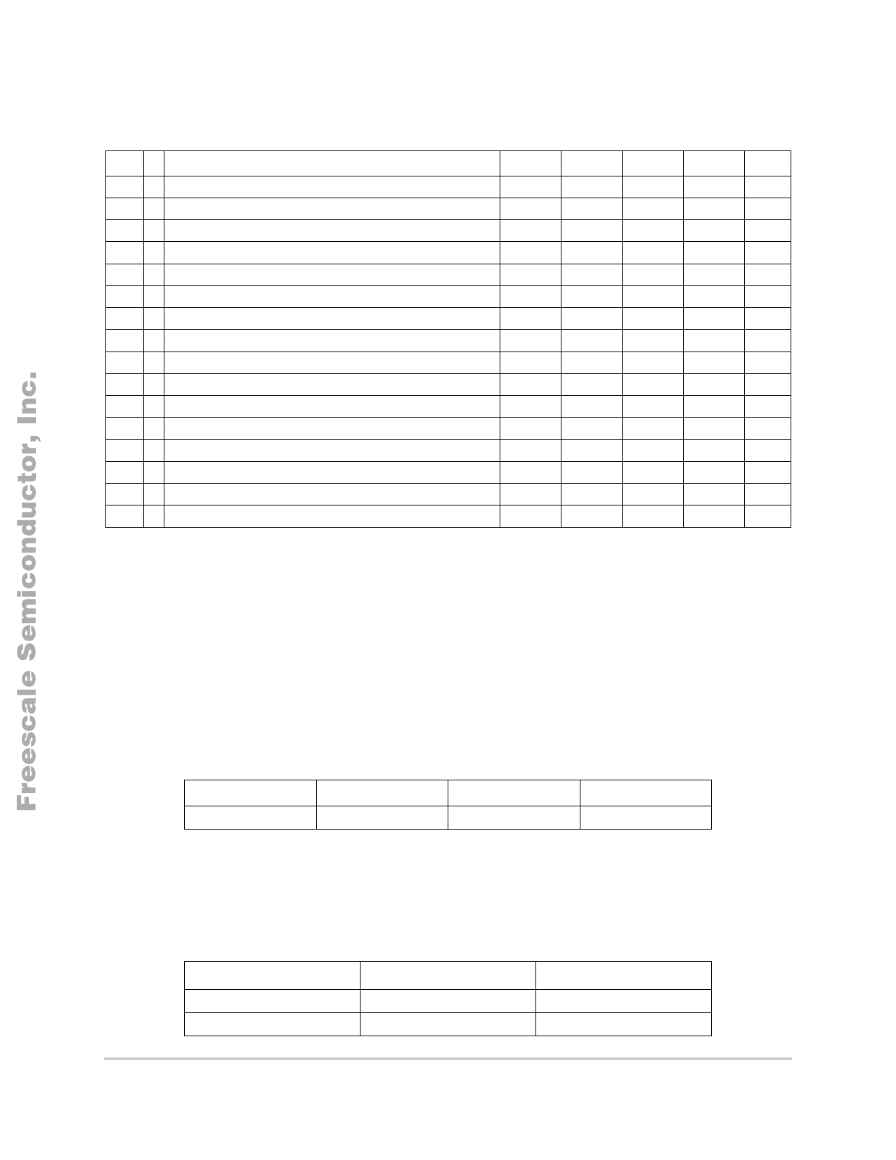
Table 18. PLL Characteristics
Num C
Rating
Symbol Min
Typ
Max Unit
J1
PLL reference frequency, crystal oscillator range 1
fREF
0.5
—
16 MHz
J2 P Self Clock Mode frequency
fSCM
1
—
5.5 MHz
J3 D VCO locking range
fVCO
8
J4 D Lock Detector transition from Acquisition to Tracking mode |∆trk|
3
J5 D Lock Detection
|∆Lock|
0
J6 D Un-Lock Detection
|∆unl|
0.5
J7 D Lock Detector transition from Tracking to Acquisition mode |∆unt|
6
J8 C PLLON Total Stabilization delay (Auto Mode) 3
tstab
—
J9 D PLLON Acquisition mode stabilization delay 3
tacq
—
J10 D PLLON Tracking mode stabilization delay 3
tal
—
—
—
—
—
—
0.5 4
0.3 5
0.2 5
40 MHz
4
%2
1.5
%2
2.5
%2
8
%2
35
ms
14
ms
24
ms
J11 D Charge pump current acquisition mode
| ich |
—
38.5
—
µA
J12 D Charge pump current tracking mode
| ich |
—
3.5
—
µA
J13 D Jitter fit VCO loop gain parameter
K1
—
–100
— MHz/V
J14 D Jitter fit VCO loop frequency parameter
J15 C Jitter fit parameter 1
J16 C Jitter fit parameter 2
f1
—
60
— MHz
j1
—
—
TBD % 4
j2
—
—
TBD % 4
1 VDDPLL at 2.5 V.
2 Percentage deviation from target frequency
3 PLL stabilization delay is highly dependent on operational requirement and external component values (for
example, crystal and XFC filter component values). Notes 4 and 5 show component values for a typical
configurations. Appropriate XFC filter values should be chosen based on operational requirement of system.
4 fREF = 4 MHz, fSYS = 25 MHz (REFDV = 0x03, SYNR = 0x01), CS = 4.7 nF, CP = 470 pF, RS = 10 KΩ.
5 fREF = 4 MHz, fSYS = 8 MHz (REFDV = 0x00, SYNR = 0x01), CS = 33 nF, CP = 3.3 nF, RS = 2.7 KΩ.
3.8.4 Crystal Monitor Time-out
The time-out Table 19 shows the delay for the crystal monitor to trigger when the clock stops, either at the high
or at the low level. The corresponding clock period with an ideal 50% duty cycle is twice this time-out value.
Table 19. Crystal Monitor Time-Outs
Min
Typ
Max
Unit
6
10
18.5
µs
3.8.5 Clock Quality Checker
The timing for the clock quality check is derived from the oscillator and the VCO frequency range in
Table 18. These numbers define the upper time limit for the individual check windows to complete.
Table 20. CRG Maximum Clock Quality Check Timings
Clock Check Windows
Value
Unit
Check Window
9.1 to 20.0
ms
Timeout Window
0.46 to 1.0
s
17
MAC7100 Microcontroller Family Hardware Specifications
MOTOROLA
PRELIMINARY—SUBJECT TO CHANGE WITHOUT NOTICE
For More Information On This Product,
Go to: www.freescale.com
Share Link: 