MAX2511 View Datasheet(PDF) - Maxim Integrated
Part Name
Description
Manufacturer
MAX2511 Datasheet PDF : 16 Pages
| |||
Low-Voltage IF Transceiver
with Limiter and RSSI
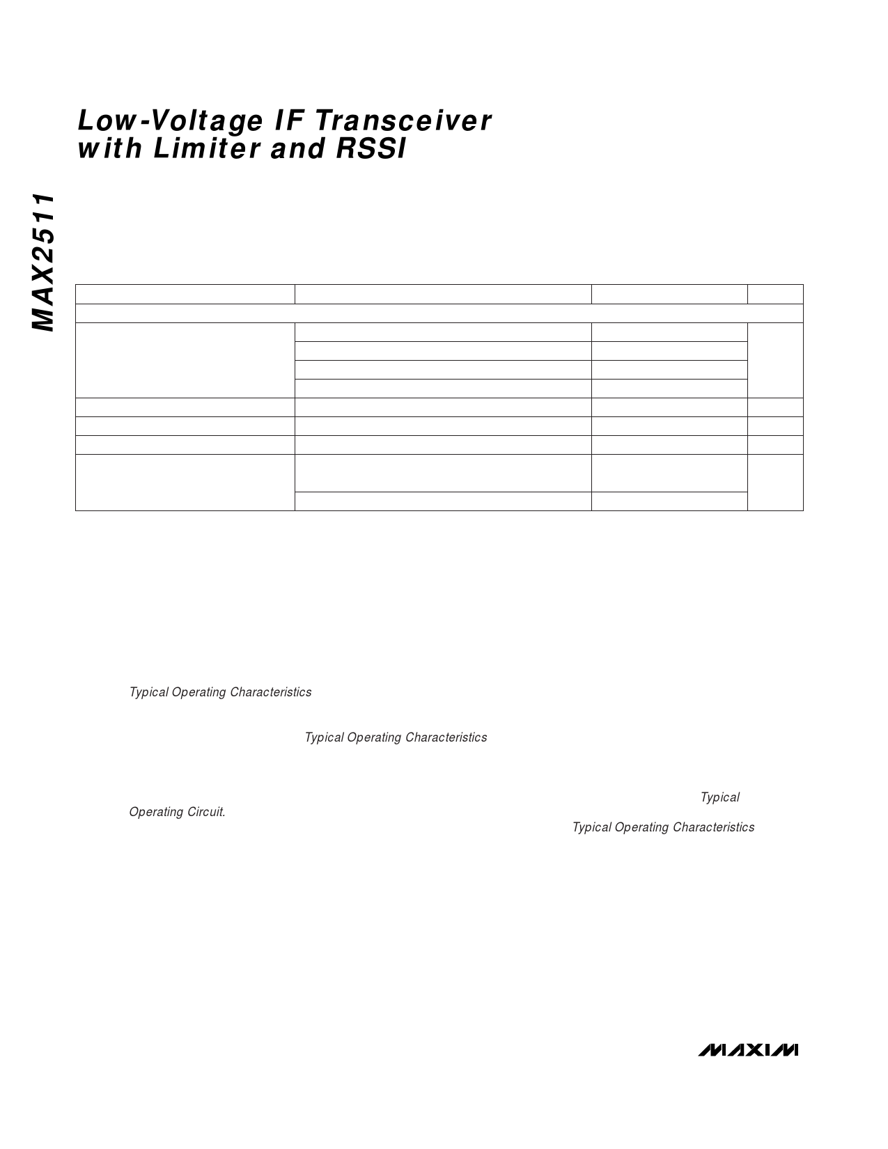
AC ELECTRICAL CHARACTERISTICS (continued)
(MAX2511 test fixture, VCC = +3.0V, RXEN = TXEN = low, 0.01µF across CZ and CZ, MIXOUT tied to VREF through 165Ω resistor,
TXIN, TXIN tied to VREF through 50Ω resistor, TXOUT and TXOUT loaded with 100Ω differential, GC open, LIMOUT, LIMOUT loaded
with 2kΩ differential, TANK and TANK driven with -2.5dBm from a 100Ω source; OSCOUT AC-terminated with 50Ω, 330pF at RSSI
pin, 0.1µF at VREF pin, Rx inputs and Tx outputs differentially coupled, PRXIN, RXIN = -28dBm (200Ω system), fRXIN, RXIN = 425MHz,
fLO = 435.7MHz, fTXIN, TXIN = 10.7MHz, TA = +25°C, unless otherwise noted.)
PARAMETER
CONDITIONS
MIN TYP MAX UNITS
TRANSMITTER (TXEN = high, VTXIN and VTXIN = 100mVp-p differential)
VGC = 0.5V, TA = +25°C
Output Power
VGC = open, TA = +25°C
VGC = 2.0V, TA = +25°C
VGC = 2.0V, TA = -40°C to +85°C (Note 1)
Image Rejection
LO Rejection
Output 1dB Compression Point
VGC = 2.0V
Output IM3 Level
0.5V < VGC < 1.87V
-40dBm < POUT < -10dBm (Note 10)
VGC = 2.0V
-44
-19
-5
-2
dBm
-6
34
25
dBc
40
30
dBc
2
dBm
-40
dBc
-35
Note 1: Guaranteed by design and characterization.
Note 2: Driving RXIN or RXIN with a power level greater than the 1dB compression level forces the input stage out of its linear
range, causing harmonic and intermodulation distortion. The RSSI output increases monotonically with increasing input
levels beyond the mixer’s 1dB compression level.
Note 3: Assuming the supply voltage has been applied, this includes settling of the limiter offset correction and the Rx or Tx bias
stabilization time. Guaranteed by design.
Note 4: LIMOUT, LIMOUT loaded with 2kΩ differential. With no load, the output swing is approximately twice as large.
Note 5: The RSSI maximum intercept is the maximum input power (over a statistical sample of parts) at which the RSSI output is 0V.
This point is extrapolated from the linear portion of the RSSI voltage versus limiter input power. This specification and the
RSSI slope define the ideal behavior of the RSSI function (the slope and intercept of a straight line), while the RSSI relative
error specification defines the deviations from this line. See the RSSI Output Voltage vs. Limiter Input Power graph in the
Typical Operating Characteristics.
Note 6: The RSSI relative error is the deviation from the best-fitting straight line of RSSI output voltage versus limiter input power.
A 0dB relative error is exactly on this line. The limiter input power range for this test is -75dBm to +5dBm from 50Ω. See the
RSSI Relative Error graph in the Typical Operating Characteristics .
Note 7: Operation outside this frequency range is possible but has not been characterized. At lower frequencies, it might be
necessary to overdrive the oscillator with an external signal source.
Note 8: If a larger output level is required, a higher value of load resistance (up to 100Ω) may be used.
Note 9: This assumes that the supply voltage has been applied, and includes the settling time of VREF, using the Typical
Operating Circuit.
Note 10: Using two tones at 10.7MHz and 10.8MHz, 50mVp-p per tone at TXIN, TXIN. See Typical Operating Characteristics.
4 _______________________________________________________________________________________
Share Link: 