MAX4295(2005) View Datasheet(PDF) - Maxim Integrated
Part Name
Description
Manufacturer
MAX4295 Datasheet PDF : 15 Pages
| |||
Mono, 2W, Switch-Mode (Class D)
Audio Power Amplifier
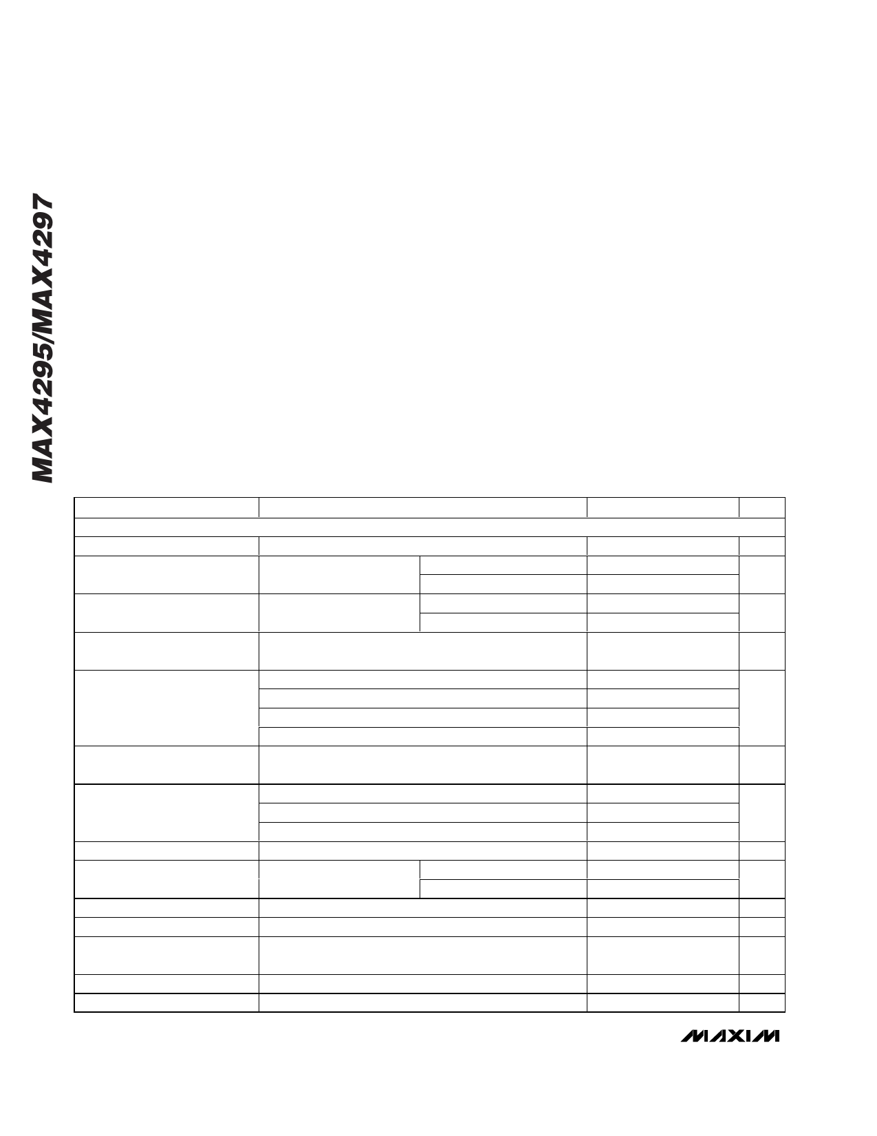
ABSOLUTE MAXIMUM RATINGS
VCC, PVCC to GND or PGND....................................-0.3V to +6V
PGND to GND.....................................................................±0.3V
PVCC to VCC .......................................................................±0.3V
VCM, SS, AOUT, IN to GND .......................-0.3V to (VCC + 0.3V)
SHDN, FS1, FS2 to GND ..........................................-0.3V to +6V
OUT_ to PGND .........................................-0.3V to (PVCC + 0.3V)
Op Amp Output Short-Circuit
Duration (AOUT).........Indefinite Short Circuit to Either Supply
H-Bridge Short-Circuit
Duration (OUT_) ................Continuous Short Circuit to PGND,
PVCC or between OUT+ and OUT-
Continuous Power Dissipation (TA = +70°C)
16-Pin QSOP (derate 8.30mW/°C above +70°C)........667mW
16-Pin Narrow SO (derate 8.7mW/°C above +70°C)......696mW
Operating Temperature Range ...........................-40°C to +85°C
Junction Temperature ......................................................+150°C
Storage Temperature Range .............................-65°C to +150°C
Lead Temperature (soldering, 10s) .................................+300°C
Stresses beyond those listed under “Absolute Maximum Ratings” may cause permanent damage to the device. These are stress ratings only, and functional
operation of the device at these or any other conditions beyond those indicated in the operational sections of the specifications is not implied. Exposure to
absolute maximum rating conditions for extended periods may affect device reliability.
ELECTRICAL CHARACTERISTICS
(VCC = PVCC = +5V, SHDN = VCC, FS1 = GND, FS2 = VCC (fOSC = 250kHz), input amplifier gain = -1V/V, TA = TMIN to TMAX, unless
otherwise noted. Typical values are TA = +25°C.) (Note 1)
PARAMETER
CONDITIONS
MIN TYP MAX UNITS
GENERAL
Supply Voltage Range
(Note 2)
2.7
5.5
V
Quiescent Supply Current
Output load not connected
2.8
4
mA
Shutdown Supply Current
SHDN = GND
1.5
8
µA
Voltage at VCM Pin
PWM Frequency
PWM Frequency Change with
VCC
Duty Cycle
Duty Cycle Change with VCC
Switch On-Resistance
(each power device)
H-Bridge Output Leakage
H-Bridge Current Limit
Soft-Start Capacitor Charging
Current
Undervoltage Lockout
Thermal Shutdown Trip Point
FS1 = GND, FS2 = GND
FS1 = GND, FS2 = VCC
FS1 = VCC, FS2 = GND
FS1 = VCC, FS2 = VCC
VCC = 2.7V to 5.5V
VIN = 0.06 × VCC
VIN = 0.30 × VCC
VIN = 0.54 × VCC
VIN = 0.3 × VCC, VCC = 2.7V to 5.5V
IOUT = 150mA
SHDN = GND
VCC = 5V
VCC = 2.7V
VSS = 0V
0.285 × 0.3 × 0.315 × V
VCC
VCC
VCC
105
125
145
210
250
290
kHz
420
500
580
840 1000 1160
±1
±3 kHz/V
10.2
12
13.8
49.2
50
50.8
%
86.2
88
89.8
±0.02 ±0.15 %/V
0.25
0.5
Ω
0.35
1.0
0
±5
µA
1
A
0.75 1.35 1.95 µA
1.8
2.2
2.6
V
145
°C
2 _______________________________________________________________________________________
Share Link: 