S25FL016A View Datasheet(PDF) - Spansion Inc.
Part Name
Description
Manufacturer
S25FL016A
Spansion Inc.

S25FL016A Datasheet PDF : 36 Pages
| |||
Data Sheet
3. Input/Output Descriptions
Signal
SO
SI
SCK
CS#
HOLD#
W#
VCC
GND
I/O
Output
Input
Input
Input
Input
Input
Input
Input
Description
Signal Data Output: Transfers data serially out of the device on the falling edge of SCK.
Serial Data Input: Transfers data serially into the device. Device latches commands, addresses,
and program data on SI on the rising edge of SCK.
Serial Clock: Provides serial interface timing. Latches commands, addresses, and data on SI on
rising edge of SCK. Triggers output on SO after the falling edge of SCK.
Chip Select: Places device in active power mode when driven low. Deselects device and places
SO at high impedance when high. After power-up, device requires a falling edge on CS# before any
command is written. Device is in standby mode when a program, erase, or Write Status Register
operation is not in progress.
Hold: Pauses any serial communication with the device without deselecting it. When driven low,
SO is at high impedance, and all input at SI and SCK are ignored. Requires that CS# also be driven
low.
Write Protect: Protects the memory area specified by Status Register bits BP2:BP0. When driven
low, prevents any program or erase command from altering the data in the protected memory area.
Supply Voltage
Ground
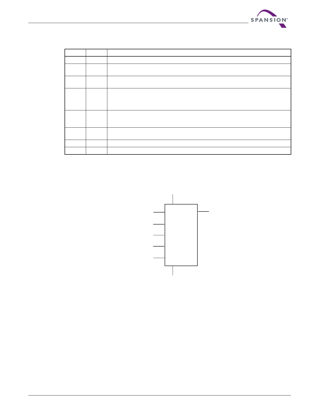
4. Logic Symbol
VCC
SI
SO
SCK
CS#
W#
HOLD#
GND
January 7, 2008 S25FL016A_00_C3
S25FL016A
9
Share Link: