NT6861 View Datasheet(PDF) - Novatek Microelectronics
Part Name
Description
Manufacturer
NT6861 Datasheet PDF : 44 Pages
| |||
NT6861
5. Timing Generator
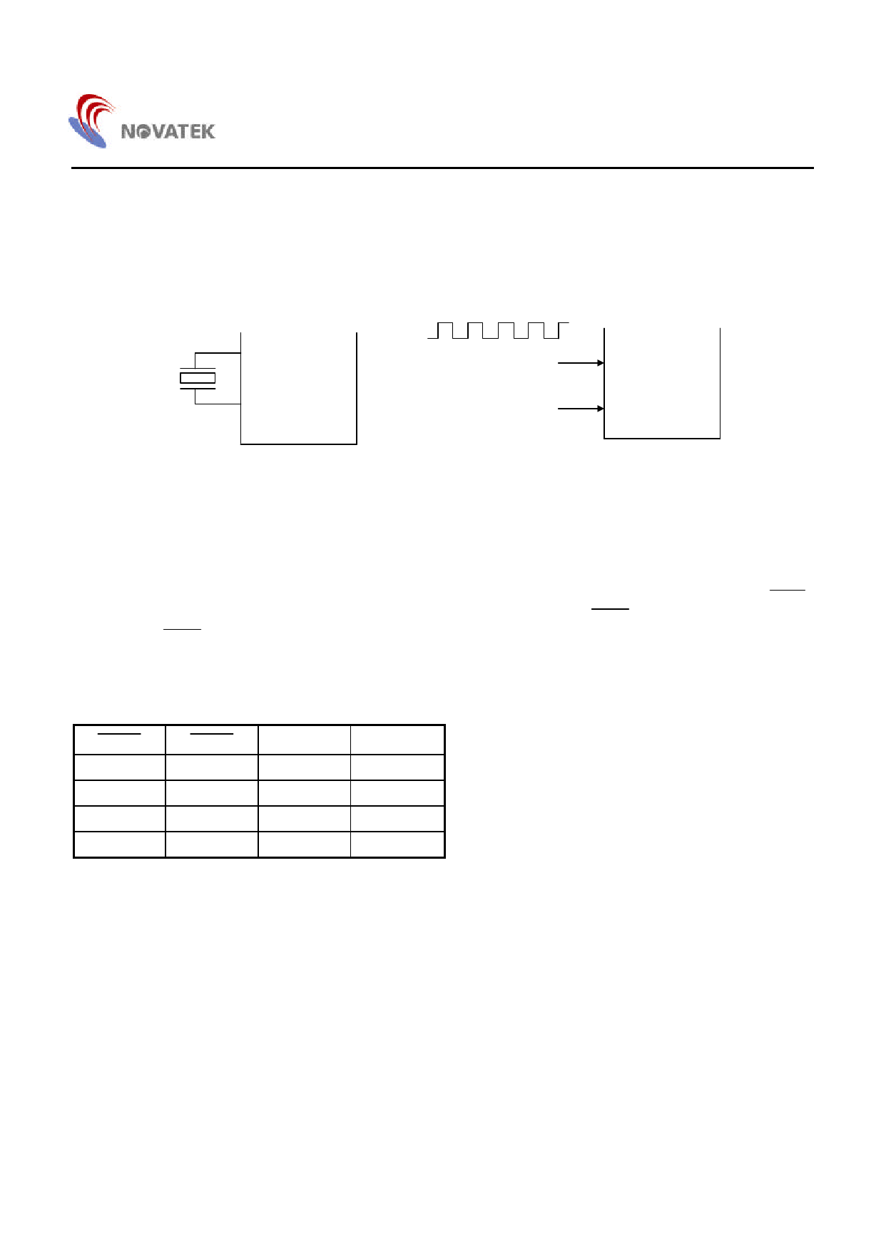
This block generates the system timing and control signal to be supplied to the CPU and on-chip peripherals. A crystal quartz,
ceramic resonator, or an external clock signal provided to the OSCI pin generates 8MHz system clock,
(4 MHz for CPU), Although internal circuits have a feedback resistor and compacitor included, components may be externally
added to ensure proper operation. The typical clock frequency is 8MHz. This frequency will affect the operation of on-chip
peripherals whose operating frequency is based on the system clock .
8MHz
OSCI
External Clock
OSCO
Unconnected
(1)
NT6861
Figure 2. Oscillator Connections
OSCI
OSCO
(2)
NT6861
6. A/D Converter
The analog to digital converter is a single 6-bit successive approximation converter. Analog voltage is supplied from external
sources to the A/D input pins and the results of the conversion are stored in the 6-bit data latch registers
($000D & $000E). The A/D converter is controlled by the control bits in the A/D control register ENDAC. Refer to the A/D
channel format table A/D input pins activation. A conversion is started by setting a '0' to the CONVERSION START bit ( CSTA )
in the A/D control register ($000D). This automatically sets the CONVERSION END bit ( CEND ) to '1'. When a conversion has
been finished, CEND bit automatically clears to '0'. The A/D conversion data in the AD LATCH registers ($000D & $000E) is
valid digital data.
The analog voltage to be measured should be stabled during the conversion operation. The variation should exceed
1/2 LSB for accuracy in measurement. Please refer Figure 3 for checking the linearity of A/D.
A/D Channel Format Table
ENAD1
0
0
1
1
ENAD0
0
1
0
1
P11 line
AD1
AD1
P11
P11
P10 line
AD0
P10
AD0
P10
11
Share Link: 