A3V56S30FTP View Datasheet(PDF) - Unspecified
Part Name
Description
Manufacturer
A3V56S30FTP Datasheet PDF : 40 Pages
| |||
A3V56S30FTP
A3V56S40FTP
256M Single Data Rate Synchronous DRAM
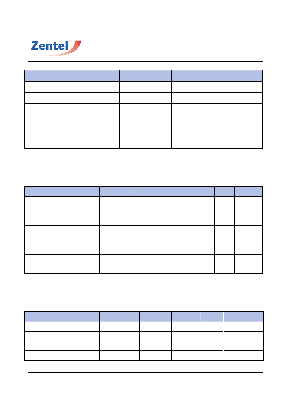
ABSOLUTE MAXIMUM RATINGS
Parameter
Symbol
Value
Unit
Voltage on any pin relative to Vss
Voltage on VDD supply relative to Vss
Storage temperature
Operating ambient temperature
Power dissipation
Short circuit current
VIN,VOUT
Vdd, VddQ
TSTG
TA
PD
IOS
-1.0 ~ 4.6
V
-1.0 ~ 4.6
V
-55 ~ +150
°C
0 ~ 70
°C
1.0
W
50
mA
NOTES:
Permanent device damage may occur if ABSOLUTE MAXIMUM RATINGS are exceeded.
Functional operation should be restricted to recommended operating condition.
Exposure to higher than recommended voltage for extended periods of time could affect device reliability.
DC OPERATING CONDITIONS
Recommended operating conditions (Voltage referenced to VSS = 0V, TA = 0 to 70°C)
Parameter
Symbol
Min
Typ
Max
Supply voltage
Vdd
3.0
3.3
3.6
VddQ
3.0
3.3
3.6
Input logic high voltage
Input logic low voltage
VIH
2.0
Vdd
Vdd + 0.3
VIL
-0.3
0
0.8
Output logic high voltage
VOH
2.4
-
-
Output logic low voltage
VOL
-
-
0.4
Input leakage current
IIL
-10
-
10
Output leakage current
IOL
-10
-
10
Unit
Note
V
V
V
1
V
2
V
IOH = -0.1mA
V
IOL = 0.1mA
uA
3
uA
3
Note:
1. VIH(max) = 4.6V AC for pulse width ≤ 10ns acceptable.
2. VIL(min) = -1.5V AC for pulse width ≤ 10ns acceptable.
3. Any input 0V ≤ VIN ≤ VDD + 0.3V, all other pins are not under test = 0V.
4. Dout is disabled , 0V ≤ VOUT ≤ VDD.
CAPACITANCE ( Vdd = VddQ = 3.3V, TA = 25°C, f = 1MHz, pin under test biased at 1.4V.)
Parameter
Symbol
Min
Max
Unit
Clock
Cclk
2
3.5
pF
/CAS,/RAS,/WE,/CS,CKE,DQMU/L
Cin
2
3.5
pF
Address
CADD
2
3.5
pF
DQ0~DQ15
COUT
3.5
5.5
pF
Note
Revision 1.1
Page 5 / 39
Mar., 2010
Share Link: 