LPC1110FD20 View Datasheet(PDF) - NXP Semiconductors.
Part Name
Description
Manufacturer
LPC1110FD20 Datasheet PDF : 59 Pages
| |||
NXP Semiconductors
LPC1111/12/13/14
32-bit ARM Cortex-M0 microcontroller
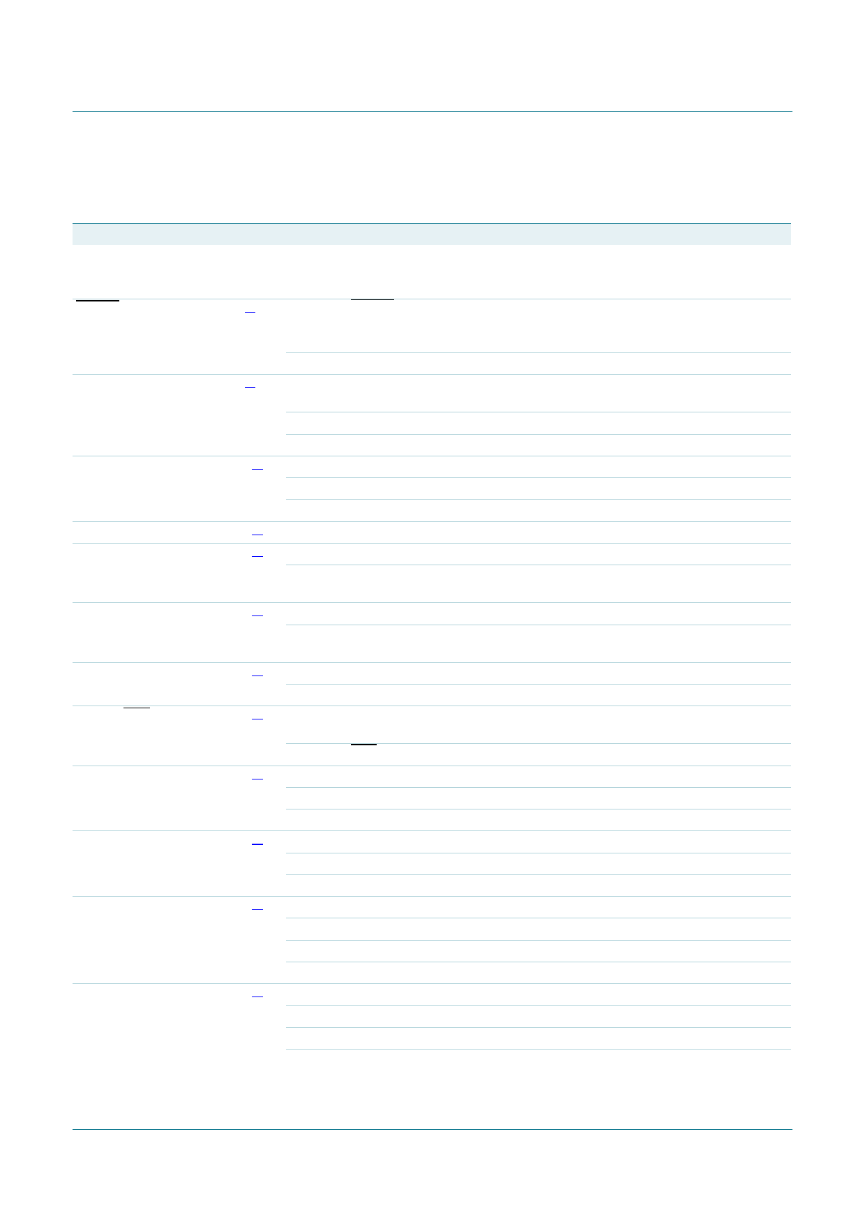
6.2 Pin description
Table 3. LPC1113/14 pin description table (LQFP48 package)
Symbol
Pin Type Description
PIO0_0 to PIO0_11
I/O
Port 0 — Port 0 is a 12-bit I/O port with individual direction and function
controls for each bit. The operation of port 0 pins depends on the function
selected through the IOCONFIG register block.
RESET/PIO0_0
3[1]
I
RESET — External reset input: A LOW on this pin resets the device,
causing I/O ports and peripherals to take on their default states, and
processor execution to begin at address 0.
I/O
PIO0_0 — General purpose digital input/output pin.
PIO0_1/CLKOUT/
CT32B0_MAT2
4[2]
I/O
PIO0_1 — General purpose digital input/output pin. A LOW level on this pin
during reset starts the ISP command handler.
O
CLKOUT — Clockout pin.
O
CT32B0_MAT2 — Match output 2 for 32-bit timer 0.
PIO0_2/SSEL0/
CT16B0_CAP0
10[2] I/O
O
PIO0_2 — General purpose digital input/output pin.
SSEL0 — Slave Select for SPI0.
I
CT16B0_CAP0 — Capture input 0 for 16-bit timer 0.
PIO0_3
14[2] I/O
PIO0_3 — General purpose digital input/output pin.
PIO0_4/SCL
15[3] I/O
PIO0_4 — General purpose digital input/output pin (open-drain).
I/O
SCL — I2C-bus, open-drain clock input/output. High-current sink only if I2C
Fast-mode Plus is selected in the I/O configuration register.
PIO0_5/SDA
16[3] I/O
PIO0_5 — General purpose digital input/output pin (open-drain).
I/O
SDA — I2C-bus, open-drain data input/output. High-current sink only if I2C
Fast-mode Plus is selected in the I/O configuration register.
PIO0_6/SCK0
22[2] I/O
PIO0_6 — General purpose digital input/output pin.
I/O
SCK0 — Serial clock for SPI0.
PIO0_7/CTS
23[2] I/O
PIO0_7 — General purpose digital input/output pin (high-current output
driver).
I
CTS — Clear To Send input for UART.
PIO0_8/MISO0/
CT16B0_MAT0
27[2] I/O
I/O
PIO0_8 — General purpose digital input/output pin.
MISO0 — Master In Slave Out for SPI0.
O
CT16B0_MAT0 — Match output 0 for 16-bit timer 0.
PIO0_9/MOSI0/
CT16B0_MAT1
28[2] I/O
I/O
PIO0_9 — General purpose digital input/output pin.
MOSI0 — Master Out Slave In for SPI0.
O
CT16B0_MAT1 — Match output 1 for 16-bit timer 0.
SWCLK/PIO0_10/
SCK0/CT16B0_MAT2
29[2] I
I/O
SWCLK — Serial wire clock.
PIO0_10 — General purpose digital input/output pin.
I/O
SCK0 — Serial clock for SPI0.
O
CT16B0_MAT2 — Match output 2 for 16-bit timer 0.
R/PIO0_11/
AD0/CT32B0_MAT3
32[4] I
I/O
R — Reserved. Configure for an alternate function in the IOCONFIG block.
PIO0_11 — General purpose digital input/output pin.
I
AD0 — A/D converter, input 0.
O
CT32B0_MAT3 — Match output 3 for 32-bit timer 0.
LPC1111_12_13_14_1
Product data sheet
All information provided in this document is subject to legal disclaimers.
Rev. 01 — 16 April 2010
© NXP B.V. 2010. All rights reserved.
8 of 59
Share Link: 