IDT7MP4120 View Datasheet(PDF) - Integrated Device Technology
Part Name
Description
Manufacturer
IDT7MP4120 Datasheet PDF : 8 Pages
| |||
IDT7MP4120
1M x 32 CMOS STATIC RAM MODULE
COMMERCIAL TEMPERATURE RANGE
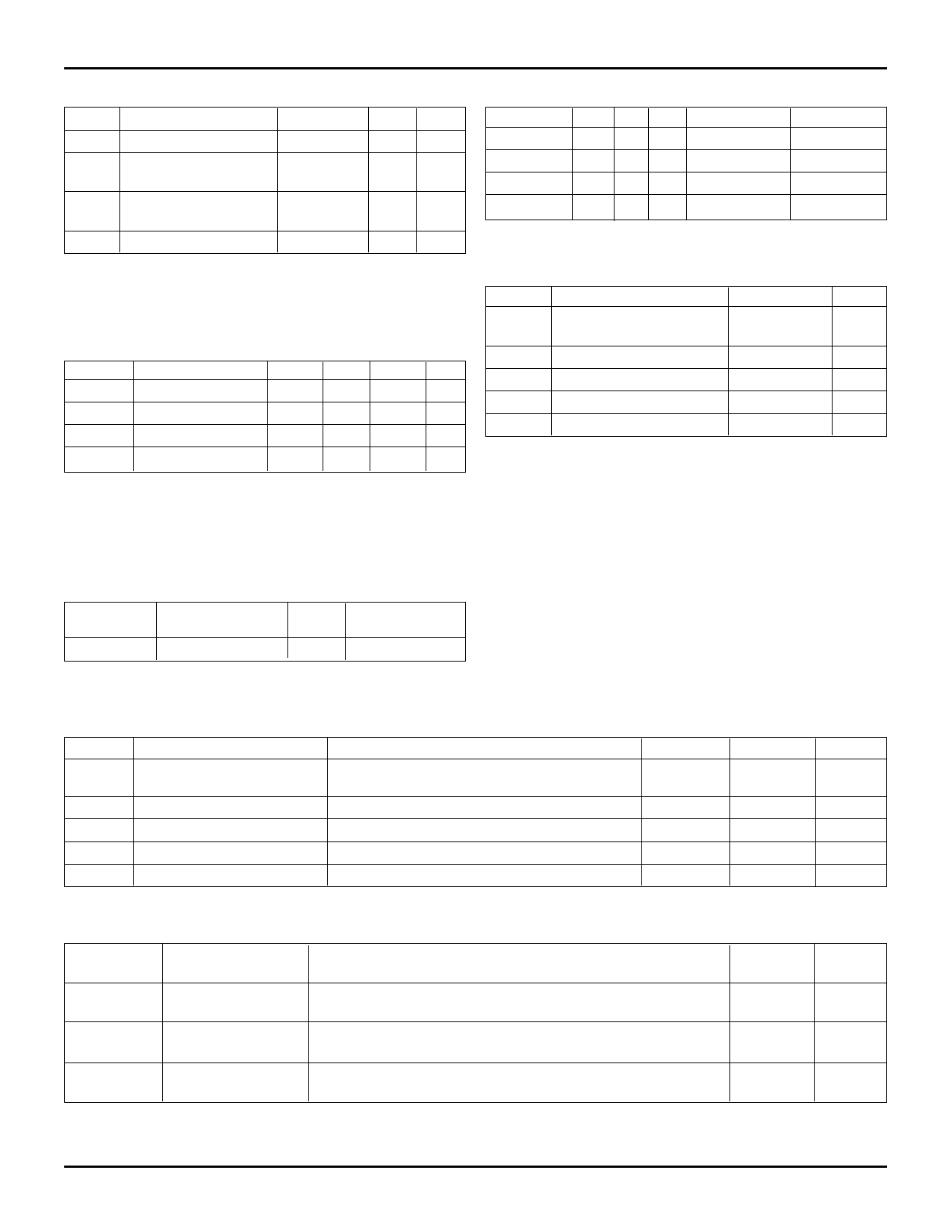
CAPACITANCE (TA = +25°C, F = 1.0MHz)
Symbol
Parameter(1)
Conditions Max. Unit
CI/O
Data I/O Capacitance V(IN) = 0V
15 pF
CIN1
Input Capacitance
(Address)
V(IN) = 0V
60 pF
CIN2 Input Capacitance
(WE, OE)
V(IN) = 0V
CIN3
Input Capacitance (CS) V(IN) = 0V
75 pF
20 pF
NOTE:
1. This parameter is guaranteed by design but not tested.
3019 tbl 02
RECOMMENDED DC OPERATING
CONDITIONS
Symbol
Parameter
Min. Typ.
VCC
Supply Voltage
4.5 5.0
GND Supply Voltage
0
0
VIH
Input High Voltage
2.2 —
VIL
Input Low Voltage –0.5(1) —
NOTE:
1. VIL (min) = –1.5V for pulse width less than 10ns.
Max. Unit
5.5 V
0
V
6.0 V
0.8 V
3019 tbl 03
RECOMMENDED OPERATING
TEMPERATURE AND SUPPLY VOLTAGE
Ambient
Grade
Temperature
GND
VCC
Commercial
0°C to +70°C
0V
5.0V ± 10%
3019 tbl 04
TRUTH TABLE
Mode CS OE WE
Standby
HXX
Read
L LH
Write
LXL
Read
L HH
Output
High-Z
DATAOUT
DATAIN
High-Z
Power
Standby
Active
Active
Active
3019 tbl 05
ABSOLUTE MAXIMUM RATINGS(1)
Symbol
Rating
Value
Unit
VTERM
Terminal Voltage with
Respect to GND
–0.5 to +7.0
V
TA
Operating Temperature
0 to +70
°C
TBIAS
Temperature Under Bias
–10 to +85
°C
TSTG
Storage Temperature
–55 to +125
°C
IOUT
DC Output Current
50
mA
NOTE:
3019 tbl 06
1. Stresses greater than those listed under ABSOLUTE MAXIMUM
RATINGS may cause permanent damage to the device. This is a stress
rating only and functional operation of the device at these or any other
conditions above those indicated in the operational sections of this
specification is not implied. Exposure to absolute maximum rating
conditions for extended periods may affect reliability.
DC ELECTRICAL CHARACTERISTICS
(VCC = 5.0V ±10%, TA = 0°C to +70°C)
Symbol
Parameter
Test Conditions
|ILI|
Input Leakage
(Address and Control)
VCC = Max.; VIN = GND to VCC
|ILI|
Input Leakage (Data)
|ILO|
Output Leakage
VCC = Max.; VIN = GND to VCC
CS VCC = Max.; = VIH, VOUT = GND to VCC
VOL
Output LOW
VCC = Min., IOL = 8mA
VOH
Output HIGH
VCC = Min., IOH = –4mA
Min.
—
—
—
—
2.4
Max.
80
10
10
0.4
—
Unit
µA
µA
µA
V
V
3019 tbl 07
Symbol
ICC
ISB
ISB1
Parameter
Dynamic Operating
Current
Standby Supply
Current
Full Standby
Supply Current
Test Conditions
f = fMAX; CS = VIL
VCC = Max.; Output Open
CS ≥ VIH, VCC = Max.
Outputs Open, f = fMAX
CS ≥ VCC – 0.2V; f = 0
VIN > VCC – 0.2V or < 0.2V
7MP4120
Max.
1280
480
120
Unit
mA
mA
mA
3019 tbl 08
7.07
2
Share Link: 