RMBA19500A-58 View Datasheet(PDF) - Raytheon Company
Part Name
Description
Manufacturer
RMBA19500A-58 Datasheet PDF : 7 Pages
| |||
Application
Information
RMBA19500A-58
PCS1900 2 Watt GaAs MMIC
Power Amplifier
ADVANCED INFORMATION
CAUTION: THIS IS AN ESD SENSITIVE DEVICE
The following describes a procedure for evaluating the RMBA19500A-58, a monolithic high efficiency
power amplifier, in a surface mount package, designed for use as a driver stage for PCS1900 Base station or as
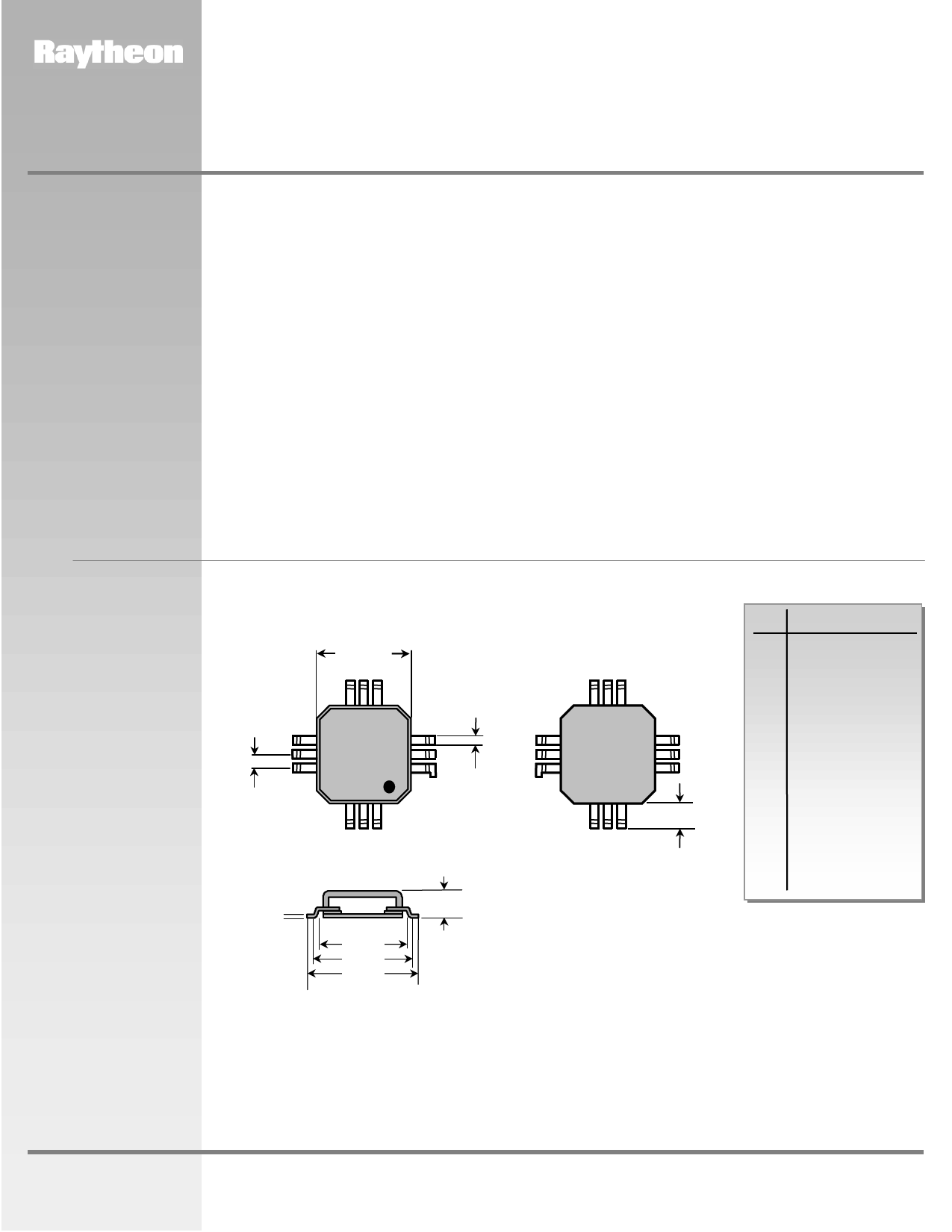
the final output stage for Micro- and Pico-Cell base stations. Figure 1 shows the package outline and the pin
designations. Figure 2 shows the functional block diagram of the packaged product. It should be noted that
RMBA19500A-58 requires external passive components for DC bias and RF output matching circuits. A
recommended schematic circuit is shown in Figure 3. The gate biases for the three stages of the amplifier may
be set by simple resistive voltage dividers. Figure 4 shows a typical layout of an evaluation board, corresponding
to the schematic circuits of figure 3. The following designations should be noted:
(1) Pin designations are as shown in figure 2.
(2) Vg1, Vg2, and Vg3 are the Gate Voltages (negative) applied at the pins of the package.
(3) Vgg1, 2, and Vgg3 are the negative supply voltages at the evaluation board terminals (Vg1 and Vg2
are tied together).
(4) Vd1, Vd2, and Vd3 are the Drain Voltages (positive) applied at the pins of the package.
(5) Vdd is the positive supply voltage at the evaluation board terminal (Vd1, Vd2, and Vd3 are tied together).
Note: The base of the package must be soldered on to a heat sink for proper operation.
Figure 1
Package Outline and
Pin Designations
Dimensions in inches
TOP VIEW
0.200 SQ.
654
BOTTOM VIEW
4 56
7
8
0.030
9
RAY
RMBA
19500A
3
3
2
0.015 2
1
1
10 1112
PLASTIC LID
0.010
0.230
0.246
0.282
0.075 MAX.
SIDE SECTION
7
8
9
12 11 10
0.041
Pin# Description
1
RF Out &Vd3
2
RF Out &Vd3
3
RF Out &Vd3
4
Vd1
5
GND
6
Vg1
7
RF In
8
GND
9
Vg2
10
Vd2
11
GND
12
Vg3
13
GND
www.raytheonrf.com
Characteristic performance data and specifications are subject to change without notice.
Revised November 14, 2001
Page 2
Raytheon RF Components
362 Lowell Street
Andover, MA 01810
Share Link: 