TDA7057Q/N1 View Datasheet(PDF) - Philips Electronics
Part Name
Description
Manufacturer
TDA7057Q/N1 Datasheet PDF : 9 Pages
| |||
Philips Semiconductors
2 x 3 W stereo BTL audio output amplifier
Objective specification
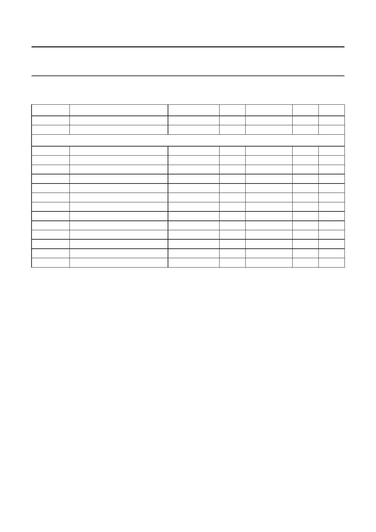
TDA7057Q
CHARACTERISTICS
VP = 11 V; f = 1 kHz; RL = 16 Ω; Tamb = 25 °C; unless otherwise specified
SYMBOL
PARAMETER
VP
IORM
positive supply voltage range
repetitive peak output current
Operating position
IP
PO
THD
total quiescent current
output power
total harmonic distortion
GV
Vno(rms)
Vno(rms)
B
voltage gain
noise output voltage (RMS value)
noise output voltage (RMS value)
bandwidth
SVRR
supply voltage ripple rejection
Voff
ZI
Ibias
α
GV
DC output offset voltage
input impedance
input bias current
channel separation
channel balance
CONDITIONS
RL = ∞; note 1
THD = 10%
PO = 0.5 W
note 2
note 3
note 4
RS = 5 kΩ
RS = 5 kΩ
MIN.
3.0
−
−
2.5
−
39
−
−
−
36
−
−
−
40
−
TYP.
11
−
MAX.
18
0.6
UNIT
V
A
10
14
mA
3
−
W
0.25
1
%
40
41
dB
180
300
µV
60
−
µV
20 Hz to 20 kHz −
60
−
dB
−
200
mV
100
−
kΩ
100
300
nA
−
−
dB
−
1
dB
Notes to the characteristics
1. With a load connected to the outputs the quiescent current will increase, the maximum value of this increase being
equal to the DC output offset voltage divided by RL.
2. The noise output voltage (RMS value) is measured with RS = 5 kΩ unweighted (20 Hz to 20 kHz).
3. The noise output voltage RMS value) at f = 500 kHz is measured with RS = 0 Ω and bandwidth = 5 kHz.
With a practical load (RL = 16 Ω, L = 200 µH) the noise output current is only 50 nA.
4. The ripple rejection is measured with RS = 0 Ω and f = 100 Hz to 10 kHz.
The ripple voltage of 200 mV (RMS value) is applied to the positive supply rail.
May 1992
6
Share Link: 