LA4525 View Datasheet(PDF) - SANYO -> Panasonic
Part Name
Description
Manufacturer
LA4525 Datasheet PDF : 8 Pages
| |||
LA4525
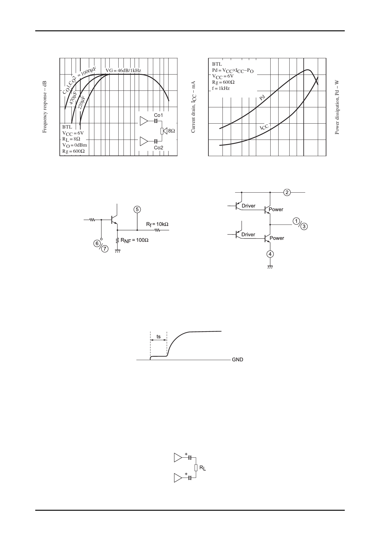
f Response
2
0
= 1000µF VG = 46dB/1kHz
-2
-4
-6
BTL
VCC = 6V
-8 RL = 8Ω
VO = 0dBm
Rg = 600Ω
-102 3 5 7100 2 3
5 7 1k 2 3 5 7 10k
Frequency, f -- Hz
+Co1
8Ω
+
Co2
2 3 5 7100k 2
JK452519
Handling Instructions and Precautions
Internal Circuits
600
ICC, Pd -- PO
1.2
BTL
Pd = VCC×ICC−PO
500 VCC = 6V
1.0
Rg = 600Ω
400 f = 1kHz
0.8
Pd
300
0.6
200
0.4
I CC
100
0.2
0
0.01
23
5 7 0.1
2 3 5 7 1.0
2 30
Output power, PO -- W
JK452520
Figure 1. Input pins (6 and 7) and BTL input pin (5)
Figure 2. Output pins (1 and 3)
External Components
• The starting time, ts, can be varied by changing the value of the input capacitor. A value of 2.2µF is recommended. A
smaller value will result in a lower starting time, and a larger value, a higher starting time.
• The output capacitor should have a value of 470µF. A lower value will cause the low-frequency roll-off and low-power
characteristics to deteriorate.
• A value of 470µF is recommended for the power supply capacitor, although this can change according to the design
setup conditions.
• In dual mode, BTL IN (the channel 2 negative feedback connection) should be left floating.
BTL mode
• The output capacitors should have a value of 470µF. If these are omitted, a ‘‘popping’’ noise occurs. Also, any output
offset will cause a current to flow which could damage the load under quiescent DC conditions.
• The output capacitors can be replaced with a single 220µF bipolar capacitor. A larger value can cause switching noise
when power is applied to the device.
No. 4022-7/8
Share Link: 