HT812D0 View Datasheet(PDF) - Holtek Semiconductor
Part Name
Description
Manufacturer
HT812D0 Datasheet PDF : 15 Pages
| |||
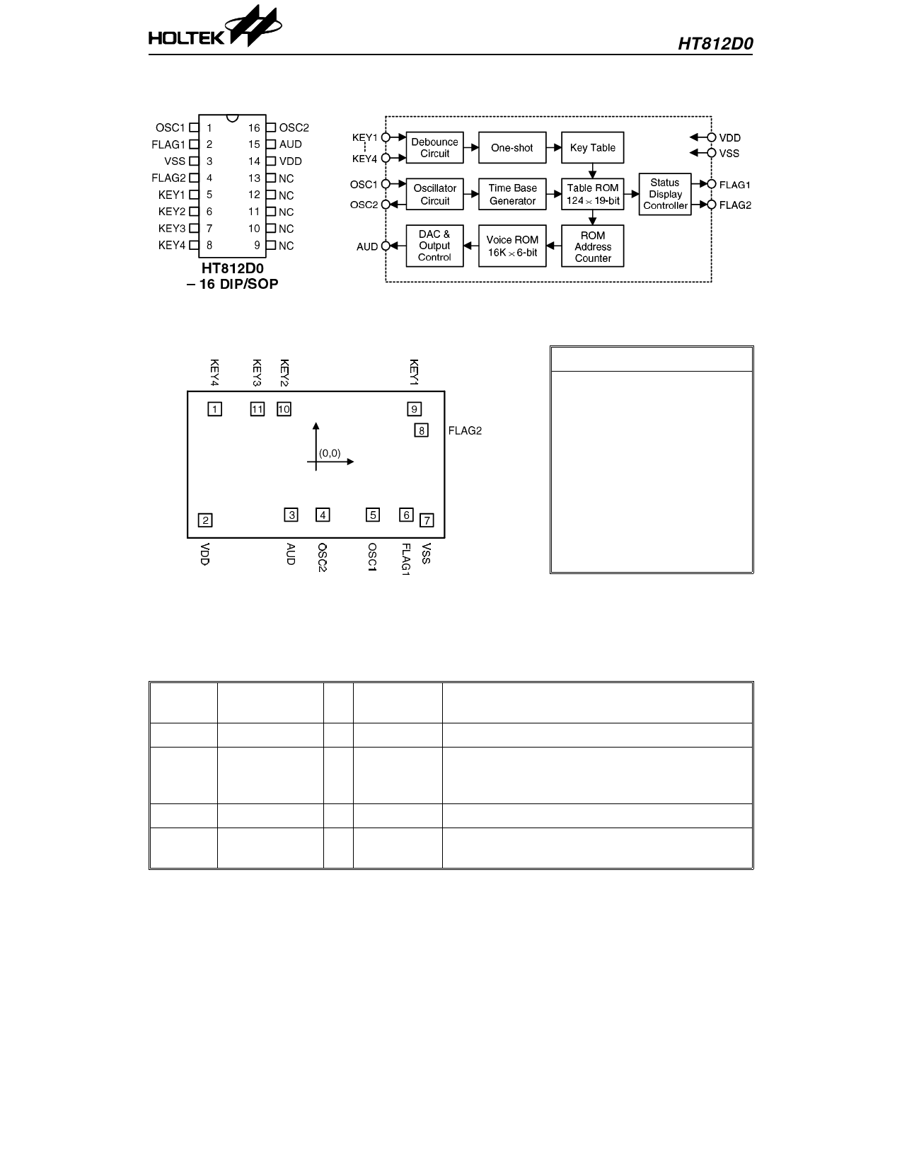
Pin Assignment
Block Diagram
HT812D0
Pad Assignment
Unit: µm
Pad No. X
1
–919.00
2
–1007.00
3
–226.99
4
61.70
5
515.20
6
821.90
7
1006.90
8
957.00
9
894.20
10 –291.90
11
–532.50
Y
480.30
–530.30
–480.30
–480.30
–480.30
–480.30
–530.30
289.10
480.30
480.30
480.30
Chip size: 2270 × 1380 (µm)2
* The IC substrate should be connected to VSS in the PCB layout artwork.
Pin Description
Pin No. Pin Name
1
OSC1
2
FLAG1
3
VSS
4
FLAG2
I/O
Internal
Connection
Description
I
—
Oscillator input pin
O
NMOS
Open Drain
3Hz/6Hz flash output, busy output, end-pulse or
voice output indication (by mask option). Open
drain, active low output
I
—
Negative power supply (GND)
O
NMOS 3Hz/6Hz flash output or busy output (by mask
Open Drain option), open drain, active low output
2
5th May ’98
Share Link: 