J505 View Datasheet(PDF) - Renesas Electronics
Part Name
Description
Manufacturer
J505 Datasheet PDF : 9 Pages
| |||
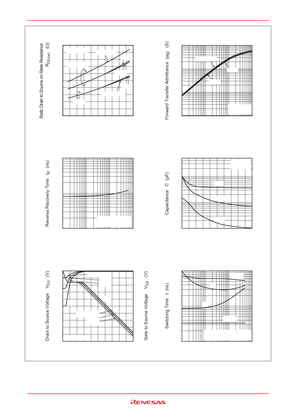
2SJ505(L), 2SJ505(S)
Static Drain to Source on State Resistance
vs. Temperature
50
Pulse Test
40
VGS = –4 V
30
ID = –50 A
–20 A
–10 A
20
10
–10 V
–50 A
–10 A, –20 A
0
–40 0
40 80 120 160
Case Temperature Tc (°C)
1000
500
Body-Drain Diode Reverse
Recovery Time
200
100
50
20
10
–0.1 –0.3 –1
di / dt = 50 A / µs
VGS = 0, Ta = 25°C
–3 –10 –30 –100
Reverse Drain Current IDR (A)
Dynamic Input Characteristics
0
0
VDD = –50 V
–25 V
–20
–10 V
–4
–40
VDS
VGS
–8
–60
VDD = –50 V
–12
–25 V
–10 V
–80
–16
ID = –50 A
–100
0
40
80
120 160
Gate Charge Qg (nc)
–20
200
Forward Transfer Admittance vs.
Drain Current
100
30
Tc = –25°C
10
25°C
3
75°C
1
0.3
VDS = –10 V
Pulse Test
0.1
–0.1 –0.3 –1 –3 –10 –30 –100
Drain Current ID (A)
50000
20000
10000
5000
Typical Capacitance vs.
Drain to Source Voltage
VGS = 0
f = 1 MHz
Ciss
2000
1000
500
Coss
200
100
0
Crss
–10 –20 –30 –40 –50
Drain to Source Voltage VDS (V)
1000
500
200
100
50
Switching Characteristics
td(off)
tf
tr
td(on)
20
10
–0.1 –0.3
VGS = –10 V, VDD = –30 V
PW = 10 µs, duty ≤ 1 %
–1 –3 –10 –30 –100
Drain Current ID (A)
Rev.5.00 Jun 05, 2006 page 4 of 8
Share Link: 