2SK2735STL-E View Datasheet(PDF) - Renesas Electronics
Part Name
Description
Manufacturer
2SK2735STL-E Datasheet PDF : 8 Pages
| |||
2SK2735(L), 2SK2735(S)
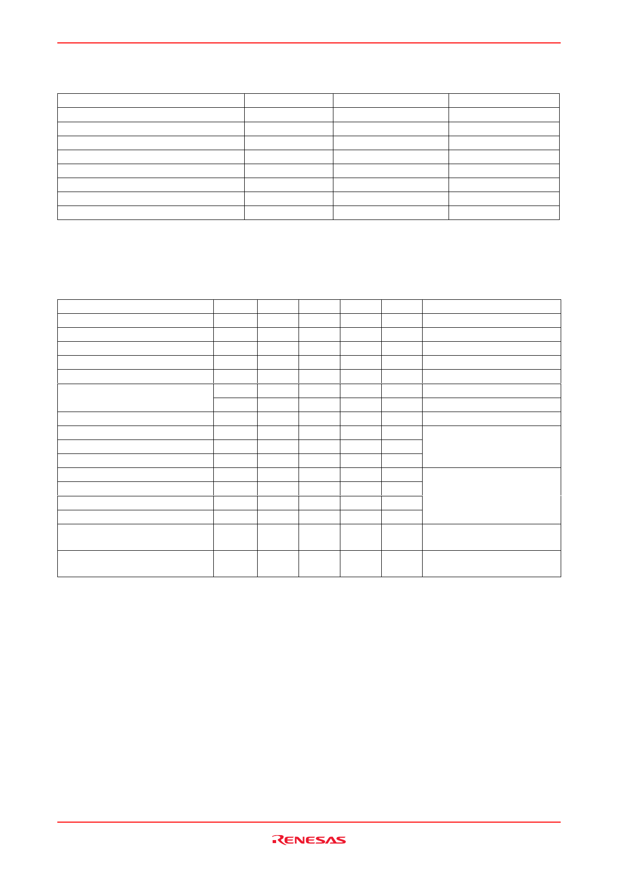
Absolute Maximum Ratings
Item
Drain to source voltage
Gate to source voltage
Drain current
Drain peak current
Body to drain diode reverse drain current
Channel dissipation
Channel temperature
Storage temperature
Notes: 1. PW ≤ 10 µs, duty cycle ≤ 1 %
2. Value at Tc = 25°C
Symbol
VDSS
VGSS
ID
ID(pulse)*1
IDR
Pch*2
Tch
Tstg
Ratings
30
±20
20
80
20
20
150
–55 to +150
(Ta = 25°C)
Unit
V
V
A
A
A
W
°C
°C
Electrical Characteristics
(Ta = 25°C)
Item
Symbol Min
Typ
Max Unit
Test Conditions
Drain to source breakdown voltage V(BR)DSS 30
—
—
V ID = 10 mA, VGS = 0
Gate to source breakdown voltage V(BR)GSS ±20
—
—
V IG = ±100 µA, VDS = 0
Gate to source leak current
IGSS
—
—
±10
µA VGS = ±16 V, VDS = 0
Zero gate voltage drain current
IDSS
—
—
10
µA VDS = 30 V, VGS = 0
Gate to source cutoff voltage
Static drain to source on state
resistance
Forward transfer admittance
VGS(off)
1.0
—
2.0
V ID = 1 mA, VDS = 10 V
RDS(on)
—
20
28
mΩ ID = 10 A, VGS = 10 V*3
RDS(on)
—
35
50
mΩ ID = 10 A, VGS = 4 V*3
|yfs|
8
16
—
S ID = 10 A, VDS = 10 V*3
Input capacitance
Ciss
—
750
—
pF VDS = 10 V, VGS = 0,
Output capacitance
Coss
—
520
—
pF f = 1 MHz
Reverse transfer capacitance
Crss
—
210
—
pF
Turn-on delay time
td(on)
—
16
—
Rise time
tr
—
225
—
Turn-off delay time
td(off)
—
85
—
Fall time
tf
—
90
—
Body to drain diode forward voltage VDF
—
1.0
—
ns ID = 10 A, VGS = 10 V,
ns RL = 1 Ω
ns
ns
V IF = 20 A, VGS = 0
diF/ dt = 50 A/ µs
Body to drain diode reverse recovery trr
time
Note: 3. Pulse test
—
40
—
V IF = 20 A, VGS = 0
diF/ dt = 50A/ µs
Rev.2.00 Sep 07, 2005 page 2 of 7
Share Link: 