2SK4115 View Datasheet(PDF) - Toshiba
Part Name
Description
Manufacturer
2SK4115 Datasheet PDF : 3 Pages
| |||
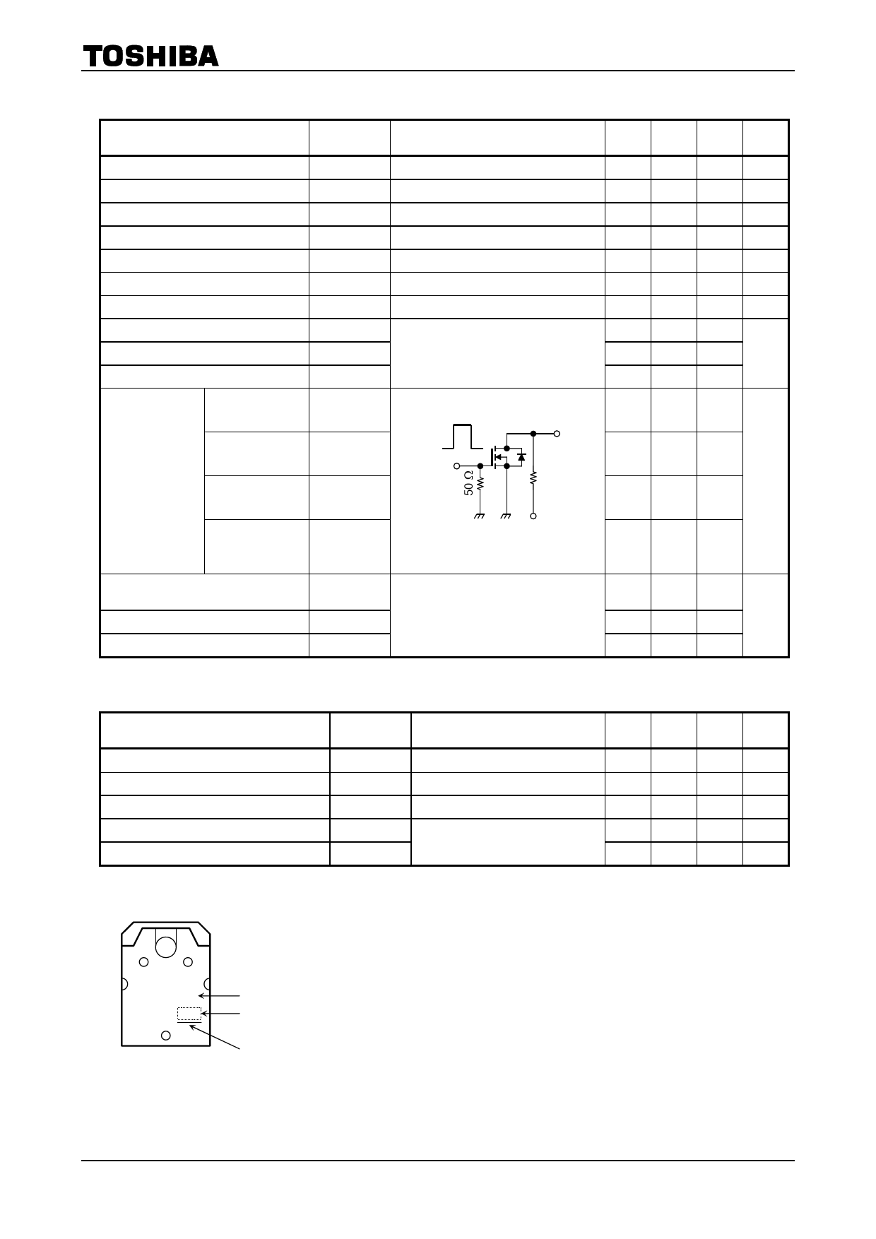
Electrical Characteristics (Ta = 25°C)
2SK4115
Characteristic
Gate leakage current
Drain-source breakdown voltage
Drain cutoff current
Drain-source breakdown voltage
Gate threshold voltage
Drain-source ON resistance
Forward transfer admittance
Input capacitance
Reverse transfer capacitance
Output capacitance
Rise time
Switching time
Turn-on time
Fall time
Turn-off time
Total gate charge
(gate-source plus gate-drain)
Gate-source charge
Gate-drain (“Miller”) charge
Symbol
Test Condition
Min Typ. Max Unit
IGSS
V (BR) GSS
IDSS
V (BR) DSS
Vth
RDS (ON)
⎪Yfs⎪
Ciss
Crss
Coss
VGS = ±30 V, VDS = 0 V
IG = ±10 μA, VDS = 0 V
VDS = 720 V, VGS = 0 V
ID = 10 mA, VGS = 0 V
VDS = 10 V, ID = 1 mA
VGS = 10 V, ID = 3.5 A
VDS = 10 V, ID = 3.5 A
VDS = 25 V, VGS = 0 V, f = 1 MHz
⎯
⎯
±10
μA
±30 ⎯
⎯
V
⎯
⎯
100
μA
900 ⎯
⎯
V
2.0
⎯
4.0
V
⎯
1.6 2.0
Ω
3.5 5.0
⎯
S
⎯ 1650 ⎯
⎯
30
⎯
pF
⎯ 140 ⎯
tr
10 V
VGS
ton
0V
tf
⎯
50
⎯
ID = 3.5 A
VOUT
⎯
90
⎯
RL = 114 Ω
ns
⎯
70
⎯
toff
Duty <= 1%, tw = 10 μs VDD ∼− 400 V
⎯ 240 ⎯
Qg
Qgs
VDD ∼− 400 V, VGS = 10 V, ID = 7 A
Qgd
⎯
45
⎯
⎯
24
⎯
nC
⎯
21
⎯
Source-Drain Ratings and Characteristics (Ta = 25°C)
Characteristic
Continuous drain reverse current (Note 1)
Pulse drain reverse current
(Note 1)
Forward voltage (diode)
Reverse recovery time
Reverse recovery charge
Symbol
IDR
IDRP
VDSF
trr
Qrr
Test Condition
⎯
⎯
IDR = 7 A, VGS = 0 V
IDR = 7 A, VGS = 0 V,
dIDR/dt = 100 A/μs
Min Typ. Max Unit
⎯
⎯
7
A
⎯
⎯
21
A
⎯
⎯
−1.7
V
⎯ 1400 ⎯
ns
⎯
12
⎯
μC
Marking
TOSHIBA
K4115
Part No. (or abbreviation code)
Lot No.
A line indicates
Lead (Pb)-Free
2
2007-07-24
Share Link: 