56F803 View Datasheet(PDF) - Freescale Semiconductor
Part Name
Description
Manufacturer
56F803 Datasheet PDF : 52 Pages
| |||
Part 2 Signal/Connection Descriptions
2.1 Introduction
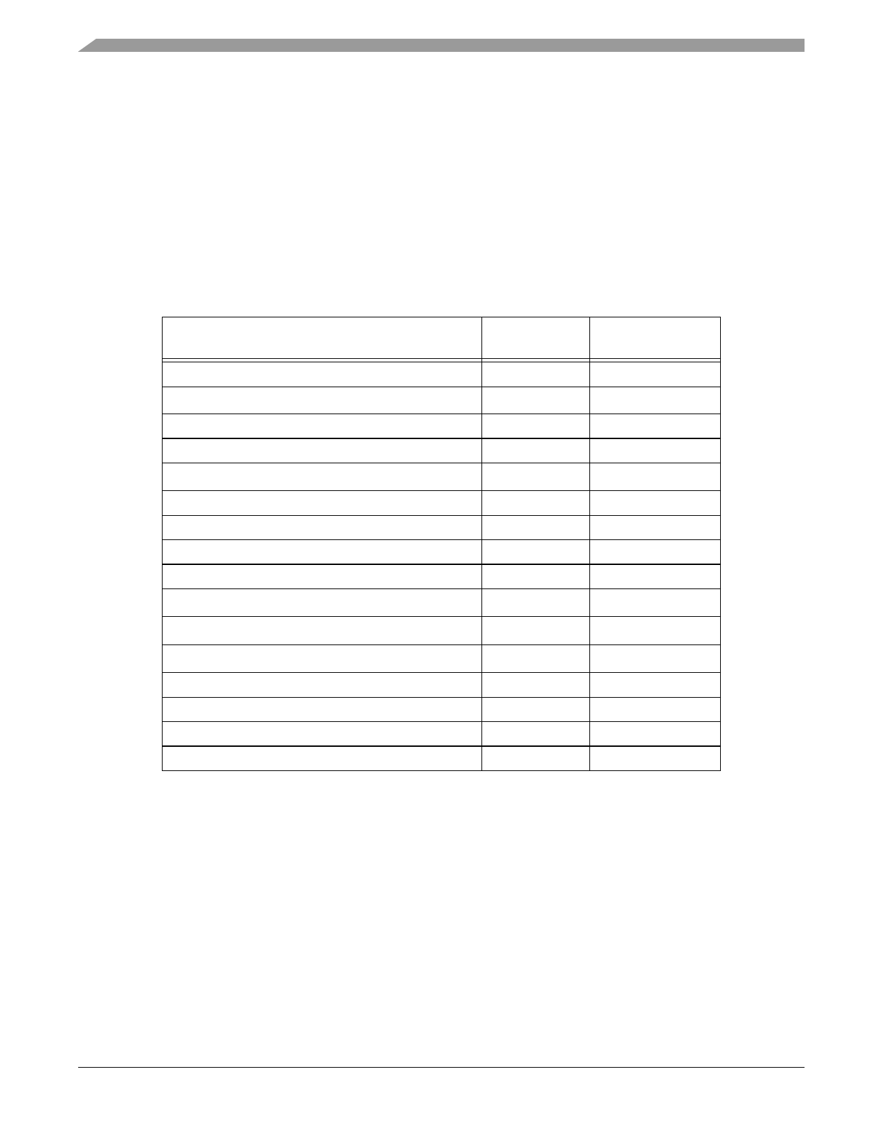
The input and output signals of the 56F803 are organized into functional groups, as shown in Table 2-1
and as illustrated in Figure 2-1. In Table 2-2 through Table 2-17, each table row describes the signal or
signals present on a pin.
Table 2-1 Functional Group Pin Allocations
Functional Group
Power (VDD or VDDA)
Ground (VSS or VSSA)
Supply Capacitors
PLL and Clock
Address Bus1
Data Bus
Bus Control
Interrupt and Program Control
Pulse Width Modulator (PWM) Port
Serial Peripheral Interface (SPI) Port1
Quadrature Decoder Port2
Serial Communications Interface (SCI) Port1
CAN Port
Analog to Digital Converter (ADC) Port
Quad Timer Module Port
JTAG/On-Chip Emulation (OnCE)
1. Alternately, GPIO pins
2. Alternately, Quad Timer pins
Number of
Pins
7
7
2
3
16
16
4
4
12
4
4
2
2
9
2
6
Detailed
Description
Table 2-2
Table 2-3
Table 2-4
Table 2-5
Table 2-6
Table 2-7
Table 2-8
Table 2-9
Table 2-10
Table 2-11
Table 2-12
Table 2-13
Table 2-14
Table 2-15
Table 2-16
Table 2-17
56F803 Technical Data, Rev. 16
8
Freescale Semiconductor
Share Link: 