74LV688D View Datasheet(PDF) - Philips Electronics
Part Name
Description
Manufacturer
74LV688D Datasheet PDF : 12 Pages
| |||
Philips Semiconductors
8-bit magnitude comparator
Product specification
74LV688
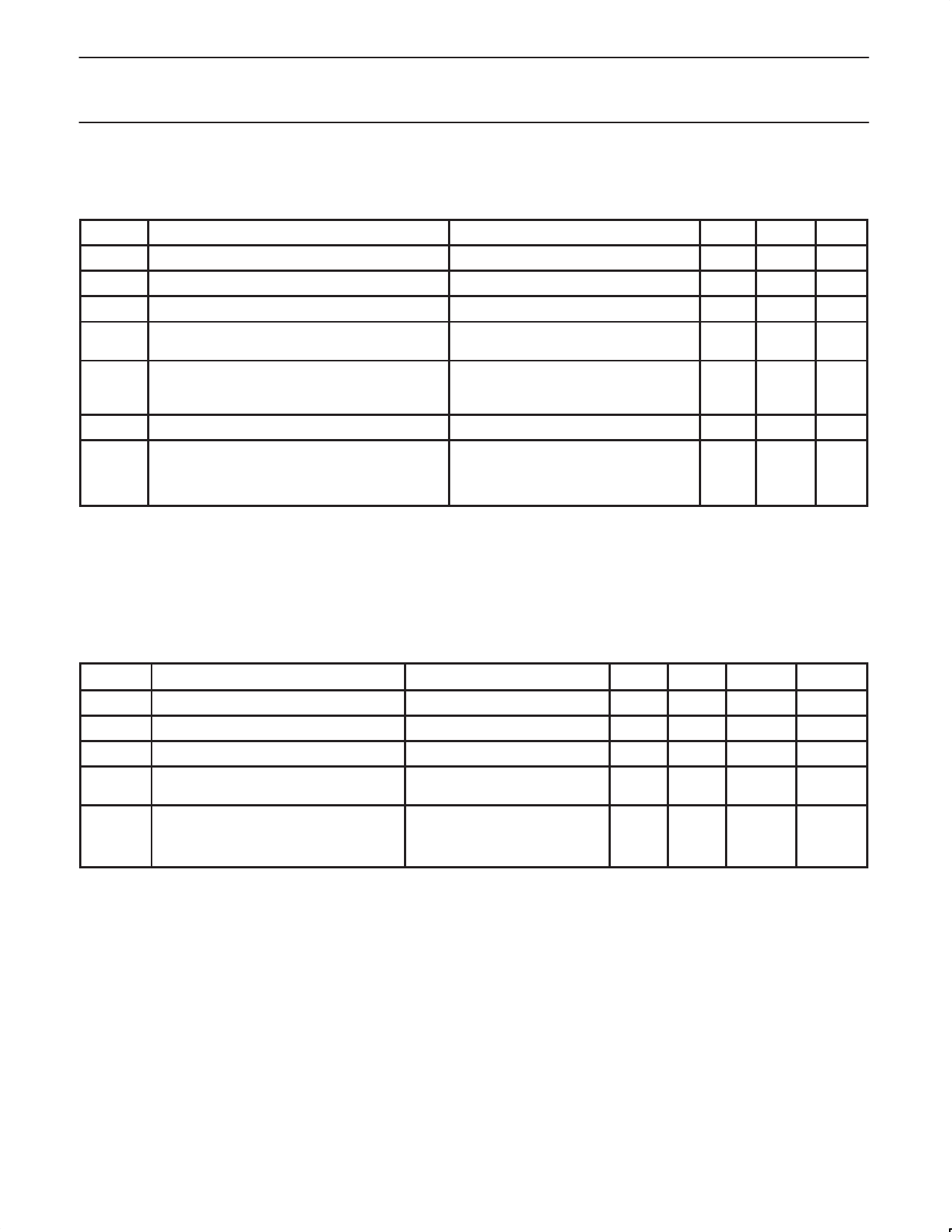
ABSOLUTE MAXIMUM RATINGS1, 2
In accordance with the Absolute Maximum Rating System (IEC 134).
Voltages are referenced to GND (ground = 0V).
SYMBOL
PARAMETER
VCC DC supply voltage
IIK
DC input diode current
IOK
DC output diode current
IO
DC output source or sink current
– standard outputs
CONDITIONS
VI < –0.5 V or V1 > VCC + 0.5V
VO < –0.5 V or V0 > VCC + 0.5V
–0.5V < VO < VCC +0.5V
MIN MAX UNIT
–0.5
+7.0
V
–
± 20
mA
–
± 50
mA
± 25
mA
± IGND,
± ICC
DC VCC or GND current for types with
– standard outputs
± 50
mA
Tstg Storage temperature range
–65
+150
°C
power dissipation per package
Ptot
– plastic DIL
– plastic mini-pack (SO)
– plastic medium-shrink SO (SSOP and TSSOP)
for temperature range: –40 to +125°C
above +70°C derate linearly with 12 mW/K
–
above +70°C derate linearly with 8 mW/K
–
above +60°C derate linearly with 5.5 mW/K
–
750
500
mW
400
NOTES:
1. Stresses beyond those listed may cause permanent damage to the device. These are stress ratings only and functional operation of the
device at these or any other conditions beyond those indicated under “recommended operating conditions” is not implied. Exposure to
absolute–maximum–rated conditions for extended periods may affect device reliability.
2. The performance capability of a high–performance integrated circuit in conjunction with its thermal environment can create junction
temperatures which are detrimental to reliability. The maximum junction temperature of this integrated circuit should not exceed 150°C.
3. The input and output negative voltage ratings may be exceeded if the input and output clamp current ratings are observed.
RECOMMENDED OPERATING CONDITIONS
SYMBOL
PARAMETER
CONDITIONS
MIN. TYP.
MAX.
UNIT
VCC
DC supply voltage
see note 1
1.0
3.3
5.5
V
VI
DC Input voltage
0
–
VCC
V
VO
DC output voltage
0
–
VCC
V
Tamb Operating ambient temperature range in
See DC and AC characteristics
–40
–
free–air
–40
–
+85
+125
°C
tr, tf
(∆t/∆v)
Input rise and fall times
VCC = 1.0V to 2.0V
VCC = 2.0V to 2.7V
VCC = 2.7V to 3.6V
VCC = 3.6V to 5.5V
–
500
–
–
200
100
ns/V
–
50
NOTE:
1. The LV is guaranteed to function down to VCC = 1.0V (input levels GND or VCC); DC characteristics are guaranteed from VCC = 1.2V to VCC = 5.5V.
1998 Jun 23
4
Share Link: 