81C55 View Datasheet(PDF) - Oki Electric Industry
Part Name
Description
Manufacturer
81C55 Datasheet PDF : 19 Pages
| |||
¡ Semiconductor
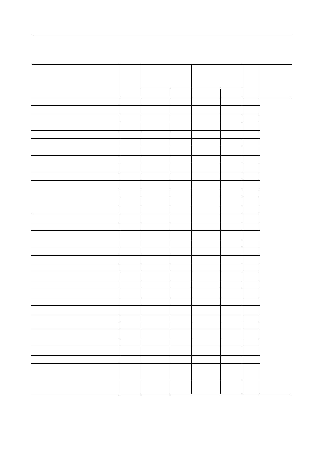
MSM81C55-5RS/GS/JS
AC CHARACTERISTICS
Parameter
VCC = 4.5 V to 5.5 V, VCC = 4.75 V to 5.25 V,
Ta = –40 to +80°C Ta = –40 to +70°C
Symbol 80C85AH 3MHz I/F 80C85AH 5MHz I/F Unit
Remarks
Min. Max. Min. Max.
Address/latch Setup Time
tAL
50
—
37
— ns
Latch/address Holt Time
tLA
30
—
30
— ns
Latch/read (write) Delay Time
tLC
100
—
40
— ns
Read/output Delay Time
tRD
—
170
—
140 ns
Address/output Delay Time
tAD
—
400
—
330 ns
Latch Width
tLL
100
—
70
— ns
Read/data Bus Floating Time
tRDF
0
100
0
80 ns
Read (write)/latch Delay Time
tCL
20
—
20
— ns
Read (write) Width
tCC
250
—
200
— ns
Data In/write Setup Time
tDW
150
—
100
— ns
Write/data-in Hold Time
tWD
0
—
25
— ns
Recovery Time
tRV
300
—
200
— ns
Write/port Output Delay Time
tWP
—
400
—
300 ns
Port Input/read Setup Time
Read/port Input Hold Time
tPR
70
—
50
— ns Load capaci-
tRP
50
—
10
— ns tance: 150 pF
Strobe/buffer Full Delay Time
tSBF
—
400
—
300 ns
Strobe Width
tSS
200
—
150
— ns
Strobe/buffer Empty Delay Time
tRBE
—
400
—
300 ns
Strobe/interrupt-on Delay Time
tSI
—
400
—
300 ns
Read/interrupt-off Delay Time
tRDI
—
400
—
300 ns
Port Input/strobe Setup Time
tPSS
50
—
20
— ns
Strobe/port-input Hold Time
tPHS
120
—
100
— ns
Strobe/buffer-empty Delay Time
tSBE
—
400
—
300 ns
Write/buffer-full Delay Time
tWBF
—
400
—
300 ns
Write/interrupt-off Delay Time
tWI
—
400
—
300 ns
Time Output Delay Time Low
tTL
—
400
—
300 ns
Time Output Delay Time High
tTH
—
400
—
300 ns
Read/data Buse Enable Delay Time
tRDE
10
—
10
— ns
Timer Cycle Time
tCYC
320
—
320
— ns
Timer Input Rise and Fall Times
tr, tf
—
80
—
80 ns
Timer Input Low Level Time
t1
80
—
40
— ns
Timer Input High Level Time
t2
120
—
70
— ns
WRITE to TIMER-IN
for writes which start counting
tWT
200
—
200
— ns
TIMER-IN to WRITE
for writes which start counting
tTW
0
—
0
— ns
Note: Timings are measured wth VL = 0.8 V and VH = 2.2 V for both input and output.
4/19
Share Link: 