PA7128 View Datasheet(PDF) - International Cmos Technology
Part Name
Description
Manufacturer
PA7128 Datasheet PDF : 6 Pages
| |||
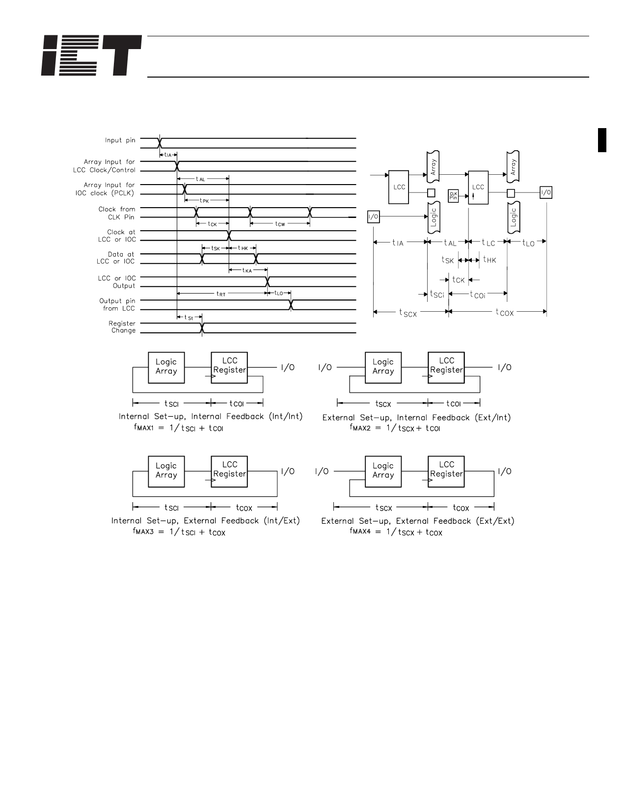
Sequential Timing - Waveforms and Block Diagram
PA7128
2
Notes:
1. Minimum DC input is -0.5V, however inputs may under-shoot to -2.0V for
periods less than 20ns.
2. Test points for Clock and VCC in tR, tF, tCL, tCH, and tRESET are referenced
at 10% and 90% levels.
3. I/O pins are 0V or VCC.
4. Test one output at a time for a duration of less than 1 sec.
5. Capacitances are tested on a sample basis.
6. Test conditions assume: signal transition times of 5ns or less from the
10% and 90% points, timing reference levels of 1.5V (unless otherwise
specified).
7. tOE is measured from input transition to VREF 0.1V (See test loads at
end of Section 6 for VREF value). tOD is measured from input transition to
VOH -0.1V or VOL +0.1V.
8. “System-clock” refers to pin 1 or pin 28 high speed clocks.
9. For T or JK registers in toggle (divide by 2) operation only.
10. For combinatorial and async-clock to LCC output delay.
11. ICC for a typical application: This parameter is tested with the device
programmed as a 10-bit D-type counter.
12. Test loads are specified in Section 5 of this Data Book.
13. “Async. clock” refers to the clock from the Sum term (OR gate).
14. The “LCC” term indicates that the timing parameter is applied to the
LCC register. The “IOC” term indicates that the timing parameter is
applied to the IOC register. The “LCC/IOC” term indicates that the tim-
ing parameter is applied to both the LCC and IOC registers. The “LCC/
IOC/INC” term indicates that the timing parameter is applied to the
LCC, IOC and INC registers.
15. This refers to the Sum-D gate routed to the IOC register for an addi-
tional buried register
16. The term “Input” without any reference to another term refers to an
(external) input pin.
17. The parameter tSPI indicates that the PCLK signal to the IOC register is
always slower than the data from the pin or input by the absolute value
of (tSK -tPK -tIA). This means that no set-up time for the data from the
pin or input is required, i.e. the external data and clock can be sent to
the device simultaneously. Additionally, the data from the pin must
remain stable for tHPI time, i.e. to wait for the PCLK signal to arrive at
the IOC register.
18. Typical (typ) ICC is measured at TA =25 o C, Freq = 25MHz, VCC =5V.
5 of 6
Share Link: 