89C535 View Datasheet(PDF) - Philips Electronics
Part Name
Description
Manufacturer
89C535 Datasheet PDF : 35 Pages
| |||
Philips Semiconductors
CMOS single-chip 8-bit microcontrollers
with FLASH program memory
Preliminary specification
89C535/89C536/89C538
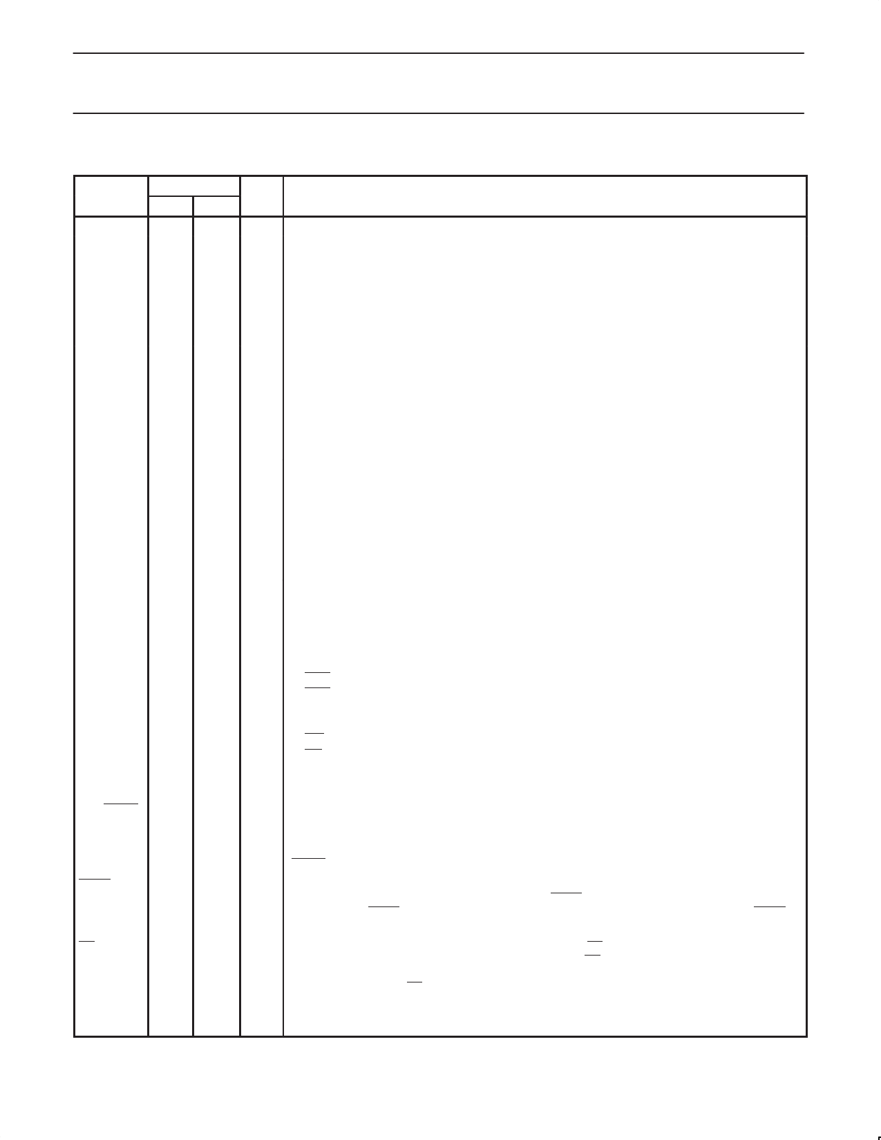
PIN DESCRIPTIONS
PIN NUMBER
MNEMONIC LCC QFP TYPE NAME AND FUNCTION
VSS
VCC
P0.0–0.7
1, 22 16, 39
23, 44 17, 38
43–36 37–30
I Ground: 0V reference.
I Power Supply: This is the power supply voltage for normal, idle, and power-down operation.
I/O Port 0: Port 0 is an open-drain, bidirectional I/O port. Port 0 pins that have 1s written to them float
and can be used as high-impedance inputs. Port 0 is also the multiplexed low-order address and
data bus during accesses to external program and data memory. In this application, it uses strong
internal pull-ups when emitting 1s. Port 0 also outputs the code bytes during program verification and
received code bytes during EEPROM programming. External pull-ups are required during program
verification.
P1.0–P1.7
2–9 40–44, I/O Port 1: Port 1 is an 8-bit bidirectional I/O port with internal pull-ups. Port 1 pins that have 1s written
1–3
to them are pulled high by the internal pull-ups and can be used as inputs. As inputs, port 1 pins that
are externally pulled low will source current because of the internal pull-ups. (See DC Electrical
Characteristics: IIL). Port 1 also receives the low-order address byte during program memory
verification.
Alternate functions for Port 1 include:
2
40
I/O
T2 (P1.0): Timer/Counter 2 external count input
3
41
I
T2EX (P1.1): Timer/Counter 2 Reload/Capture
P2.0–P2.7
24–31 18–25
I/O Port 2: Port 2 is an 8-bit bidirectional I/O port with internal pull-ups. Port 2 pins that have 1s written
to them are pulled high by the internal pull-ups and can be used as inputs. As inputs, port 2 pins that
are externally being pulled low will source current because of the internal pull-ups. (See DC
Electrical Characteristics: IIL). Port 2 emits the high-order address byte during fetches from external
program memory and during accesses to external data memory that use 16-bit addresses (MOVX
@DPTR). In this application, it uses strong internal pull-ups when emitting 1s. Some Port 2 pins
receive the high order address bits during EEPROM programming and verification.
P3.0–P3.7 11,
5,
13–19 7–13
11
5
13
7
14
8
15
9
16
10
17
11
18
12
19
13
I/O Port 3: Port 3 is an 8-bit bidirectional I/O port with internal pull-ups. Port 3 pins that have 1s written
to them are pulled high by the internal pull-ups and can be used as inputs. As inputs, port 3 pins that
are externally being pulled low will source current because of the pull-ups. (See DC Electrical
Characteristics: IIL). Port 3 also serves the special features of the 80C51 family, as listed below:
I
RxD (P3.0): Serial input port
O
TxD (P3.1): Serial output port
I
INT0 (P3.2): External interrupt
I
INT1 (P3.3): External interrupt
I
T0 (P3.4): Timer 0 external input
I
T1 (P3.5): Timer 1 external input
O
WR (P3.6): External data memory write strobe
O
RD (P3.7): External data memory read strobe
RST
10
4
I Reset: A high on this pin for two machine cycles while the oscillator is running, resets the device. An
internal diffused resistor to VSS permits a power-on reset using only an external capacitor to VCC.
ALE/PROG 33
27
O Address Latch Enable/Program Pulse: Output pulse for latching the low byte of the address
during an access to external memory. In normal operation, ALE is emitted at a constant rate of 1/6
the oscillator frequency, and can be used for external timing or clocking. Note that one ALE pulse is
skipped during each access to external data memory. This pin is also the program pulse input
(PROG) during EEPROM programming.
PSEN
32
26
O Program Store Enable: The read strobe to external program memory. When the processor is
executing code from the external program memory, PSEN is activated twice each machine cycle,
except that two PSEN activations are skipped during each access to external data memory. PSEN is
not activated during fetches from internal program memory.
EA/VPP
35
29
I External Access Enable/Programming Supply Voltage: EA must be externally held low to enable
the device to fetch code from external program memory. If EA is held high, the device executes from
internal program memory. This pin also receives the 12V programming supply voltage (VPP) during
EPROM programming. EA is internally latched on Reset.
XTAL1
21
15
I Crystal 1: Input to the inverting oscillator amplifier and input to the internal clock generator circuits.
XTAL2
20
14
O Crystal 2: Output from the inverting oscillator amplifier.
NOTE:
To avoid “latch-up” effect at power-on, the voltage on any pin at any time must not be higher than VCC + 0.5V or VSS – 0.5V, respectively.
1997 Jun 05
5
Share Link: 