89C4051 View Datasheet(PDF) - Atmel Corporation
Part Name
Description
Manufacturer
89C4051 Datasheet PDF : 19 Pages
| |||
AT89C4051
Program Verify: If lock bits LB1 and LB2 have not been programmed code data can be read
back via the data lines for verification:
1. Reset the internal address counter to 000H by bringing RST from “L” to “H”.
2. Apply the appropriate control signals for Read Code data and read the output data at
the port P1 pins.
3. Pulse pin XTAL1 once to advance the internal address counter.
4. Read the next code data byte at the port P1 pins.
5. Repeat steps 3 and 4 until the entire array is read.
The lock bits cannot be verified directly. Verification of the lock bits is achieved by observing that
their features are enabled.
Chip Erase: The entire PEROM array (4K bytes) and the two Lock Bits are erased electrically
by using the proper combination of control signals and by holding P3.2 low for 10 ms. The code
array is written with all “1”s in the Chip Erase operation and must be executed before any non-
blank memory byte can be re-programmed.
Reading the Signature Bytes: The signature bytes are read by the same procedure as a nor-
mal verification of locations 000H, 001H, and 002H, except that P3.5 and P3.7 must be pulled to
a logic low. The values returned are as follows.
(000H) = 1EH indicates manufactured by Atmel
(001H) = 41H indicates AT89C4051
13. Programming Interface
Every code byte in the Flash array can be written and the entire array can be erased by using
the appropriate combination of control signals. The write operation cycle is self-timed and once
initiated, will automatically time itself to completion.
Most major worldwide programming vendors offer support for the Atmel AT89 microcontroller
series. Please contact your local programming vendor for the appropriate software revision.
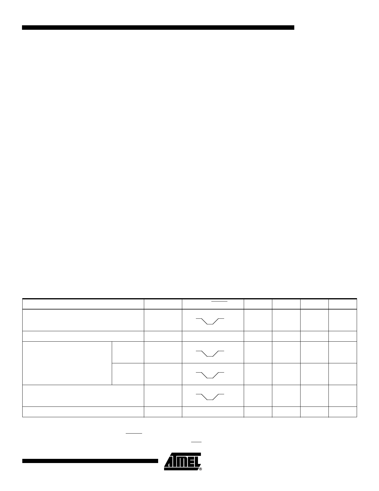
13.1 Flash Programming Modes
Mode
RST/VPP
P3.2/PROG
P3.3
P3.4
P3.5
P3.7
Write Code Data(1)(3)
12V
L
H
H
H
Read Code Data(1)
H
H
L
L
H
H
Write Lock
Bit - 1
12V
Bit - 2
12V
H
H
H
H
H
H
L
L
Chip Erase
12V
(2)
H
L
L
L
Read Signature Byte
H
H
L
L
L
L
Notes: 1. The internal PEROM address counter is reset to 000H on the rising edge of RST and is advanced by a positive pulse at
XTAL1 pin.
2. Chip Erase requires a 10-ms PROG pulse.
3. P3.1 is pulled Low during programming to indicate RDY/BSY.
9
1001E–MICRO–6/05
Share Link: 