A8351601 View Datasheet(PDF) - AMIC Technology
Part Name
Description
Manufacturer
A8351601 Datasheet PDF : 44 Pages
| |||
A8351601 Series
Operating Description
The detail description of the A8351601 included in this
description are:
n Memory Map and Registers
n Timer/Counters
n Serial Interface
n Interrupt System
n Other Information
Memory Map and Registers
Memory
The A8351601 has separate address spaces for program
and data memory. The program and data memory can be
up to 64K bytes.
The A8351601 has 256 bytes of on-chip RAM, plus
numbers of special function registers. The lower 128 bytes
can be accessed either by direct addressing or by indirect
addressing. The upper 128 bytes can be accessed by
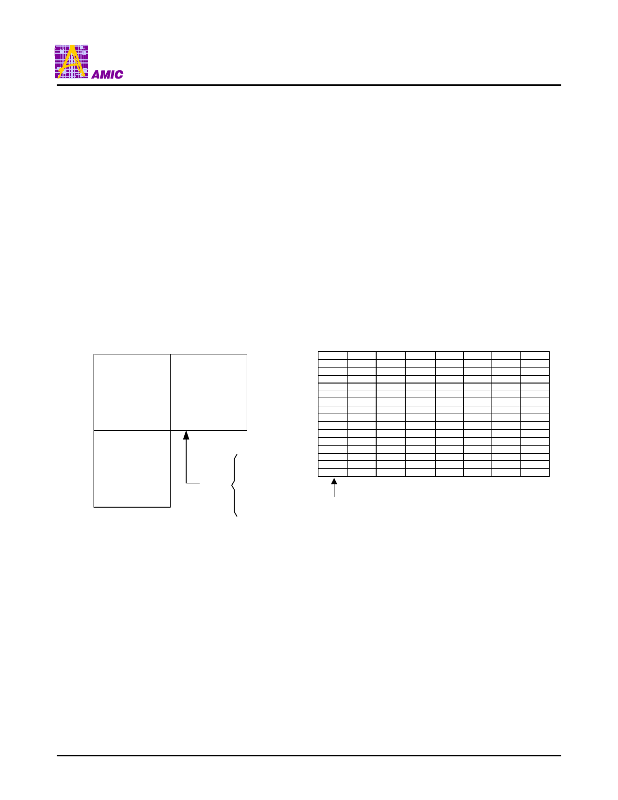
indirect addressing only. Figure 1 shows internal data
memory organization and SFR Memory Map.
FFH
Upper
128
80H
7FH
Lower
128
0
Accessible
by Indirect
Addressing
Only
Accessible
by Direct
and Indirect
Addressing
FFH
Accessible
by Direct
Addressing
80H
Special
Function
Registers
Ports,
Status and
Control Bits,
Timer,
Registers,
Stack Pointer,
Accumulator
(Etc.)
The lower 128 bytes of RAM can be divided into three
segments as listed below.
1. Register Banks 0-3: locations 00H through 1FH (32
bytes). The device after reset defaults to register bank 0.
To use the other register banks, the user must select
them in software. Each register bank contains eight 1-
byte registers R0-R7. Reset initializes the stack point to
location 07H, and is incremented once to start from 08H,
which is the first register of the second register bank.
2. Bit Addressable Area: 16 bytes have been assigned for
this segment 20H-2FH. Each one of the 128 bits of this
segment can be directly addressed (0-7FH). Each of the
16 bytes in this segment can also be addressed as a
byte.
3. Scratch Pad Area: 30H-7FH are available to the user as
data RAM. However, if the data pointer has been
initialized to this area, enough bytes should be left aside
to prevent SP data destruction.
Special Function Registers
The Special Function Registers (SFR's) are located in
upper 128 Bytes direct addressing area. The SFR Memory
Map in Figure 1 shows that.
F8
F0 B
E8
E0 ACC
D8
D0 PSW
C8 T2CON
RCAP2L RCAP2H TL2 TH2
C0
B8 IP
B0 P3
A8 IE
A0 P2
ADD PWM1 PWM2
98 SCON SBUF
90 P1
88 TCON TMOD TL0
TL1
TH0
TH1
80 P0
SP
DPL
DPH
FF
F7
EF
E7
DF
D7
CF
C7
BF
B7
AF
A7
9F
97
8F
PCON 87
Bit
Addressable
Figure 1. Internal Data Memory and SFR Memory Map
Not all of the addresses are occupied. Unoccupied
addresses are not implemented on the chip. Read
accesses to these addresses in general return random
data, and write accesses have no effect.
User software should not write 1s to these unimplemented
locations, since they may be used in future
microcontrollers to invoke new features. In that case, the
reset or inactive values of the new bits will always be 0, and
their active values will be 1.
The functions of the SFRs are outlined in the following
sections.
Accumulator (ACC)
ACC is the Accumulator register. The mnemonics for
Accumulator-specific instructions, however, refer to the
Accumulator simply as A.
B Register (B)
The B register is used during multiply and divide
operations. For other instructions it can be treated as
another scratch pad register.
(July, 2002, Version 1.0)
6
AMIC Technology, Inc.
Share Link: 