AD1836A View Datasheet(PDF) - Analog Devices
Part Name
Description
Manufacturer
AD1836A Datasheet PDF : 24 Pages
| |||
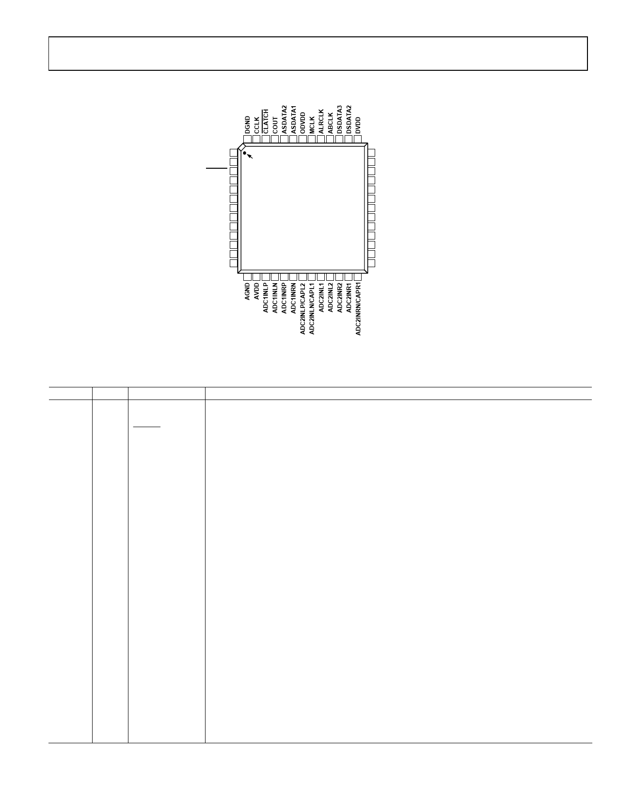
PIN CONFIGURATION AND PIN FUNCTIONAL DESCRIPTIONS
52 51 50 49 48 47 46 45 44 43 42 41 40
DVDD 1
CDATA 2
PD/RST 3
OUTLP3 4
OUTLN3 5
OUTLP2 6
OUTLN2 7
OUTLP1 8
OUTLN1 9
AVDD 10
AGND 11
FILTD 12
FILTR 13
PIN 1
IDENTIFIER
AD1836A
TOP VIEW
(Not to Scale)
39 DGND
38 DSDATA1
37 DBCLK
36 DLRCLK
35 OUTRP3
34 OUTRN3
33 OUTRP2
32 OUTRN2
31 OUTRP1
30 OUTRN1
29 AGND
28 AGND
27 ADC2INRP/CAPR2
14 15 16 17 18 19 20 21 22 23 24 25 26
AD1836A
Figure 2. 52-Lead MQFP
Table 10. Pin Function Descriptions—52-Lead MQFP
Pin No. In/Out Mnemonic
Description
1
I
DVDD
Digital Power Supply. Connect to digital 5 V supply.
2
I
CDATA
Serial Control Input.
3
I
PD/RST
Power-Down Reset (Active Low).
4
O
OUTLP3
DAC 3 Left Positive Output.
5
O
OUTLN3
DAC 3 Left Negative Output.
6
O
OUTLP2
DAC 2 Left Positive Output.
7
O
OUTLN2
DAC 2 Left Negative Output.
8
O
OUTLP1
DAC 1 Left Positive Output.
9
O
OUTLN1
DAC 1 Left Negative Output.
10
I
AVDD
Analog Power Supply. Connect to analog 5 V.
11
I
AGND
Analog Ground.
12
I
FILTD
Filter Capacitor Connection. Bypass with 10 µF||100 nF to AGND.
13
I
FILTR
Voltage Reference Filter Capacitor Connection. Bypass with 10 µF||100 nF to AGND.
14
I
AGND
Analog Ground.
15
I
AVDD
Analog Power Supply. Connect to analog 5 V supply.
16
I
ADC1INLP
ADC1 Left Positive Input.
17
I
ADC1INLN
ADC1 Left Negative Input.
18
I
ADC1INRP
ADC1 Right Positive Input.
19
I
ADC1INRN
ADC1 Right Negative Input.
20
I
ADC2INLP/CAPL2 ADC2 Left Positive Input (Direct Mode)/ADC2 Left Decoupling Cap (MUX/PGA and PGA Differential Mode).
21
I
ADC2INLN/CAPL1 ADC2 Left Negative Input (Direct Mode)/ADC2 Left Decoupling Capacitor
(MUX/PGA and PGA Differential Mode).
22
I
ADC2INL1
ADC2 Left Input 1 (MUX/PGA Mode)/Left Positive Input (PGA Differential Mode).
23
I
ADC2INL2
ADC2 Left Input 2 (MUX/PGA Mode)/Left Negative Input (PGA Differential Mode).
24
I
ADC2INR2
ADC2 Right Input 2 (MUX/PGA Mode)/Right Negative Input (PGA Differential Mode).
25
I
ADC2INR1
ADC2 Right Input 1 (MUX/PGA Mode)/Right Positive Input (PGA Differential Mode).
26
I
ADC2INRN/CAPR1 ADC2 Right Negative Input (Direct Mode)/ADC2 Right Decoupling Capacitor
(MUX/PGA and PGA Differential Mode).
Rev. 0 | Page 9 of 24
Share Link: 