AD5171 View Datasheet(PDF) - Analog Devices
Part Name
Description
Manufacturer
AD5171 Datasheet PDF : 24 Pages
| |||
PIN CONFIGURATION AND FUNCTION DESCRIPTIONS
AD5171
W1
8A
VDD 2 AD5171 7 B
TOP VIEW
GND 3 (Not to Scale) 6 AD0
SCL 4
5 SDA
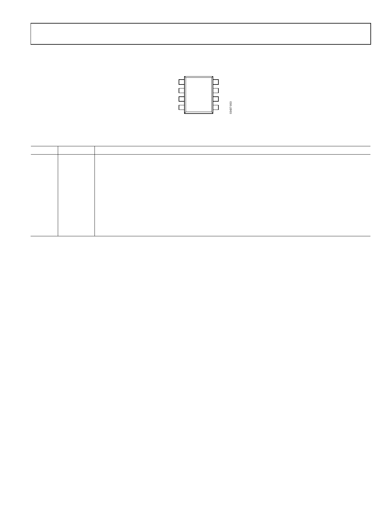
Figure 4. Pin Configuration
Table 4. Pin Function Descriptions
Pin No. Mnemonic Description
1
W
Wiper Terminal W. GND ≤ VW ≤ VDD.
2
VDD
Positive Power Supply. Specified for operation from 2.7 V to 5.5 V. For OTP programming, VDD needs to be within
the 4.75 V and 5.25 V range and capable of driving 100 mA.
3
GND
Common Ground.
4
SCL
Serial Clock Input. Requires a pull-up resistor. If it is driven direct from a logic controller without the pull-up
resistor, ensure that the VIH minimum is 0.7 V × VDD.
5
SDA
6
AD0
Serial Data Input/Output. Requires a pull-up resistor. If it is driven direct from a logic controller without a pull-up
resistor, ensure that the VIH minimum is 0.7 V × VDD.
I2C Device Address Bit. Allows a maximum of two AD5171s to be addressed.
7
B
Resistor Terminal B. GND ≤ VB ≤ VDD.
8
A
Resistor Terminal A. GND ≤ VA ≤ VDD.
Rev. D | Page 7 of 24
Share Link: 