AD542 View Datasheet(PDF) - Analog Devices
Part Name
Description
Manufacturer
AD542 Datasheet PDF : 12 Pages
| |||
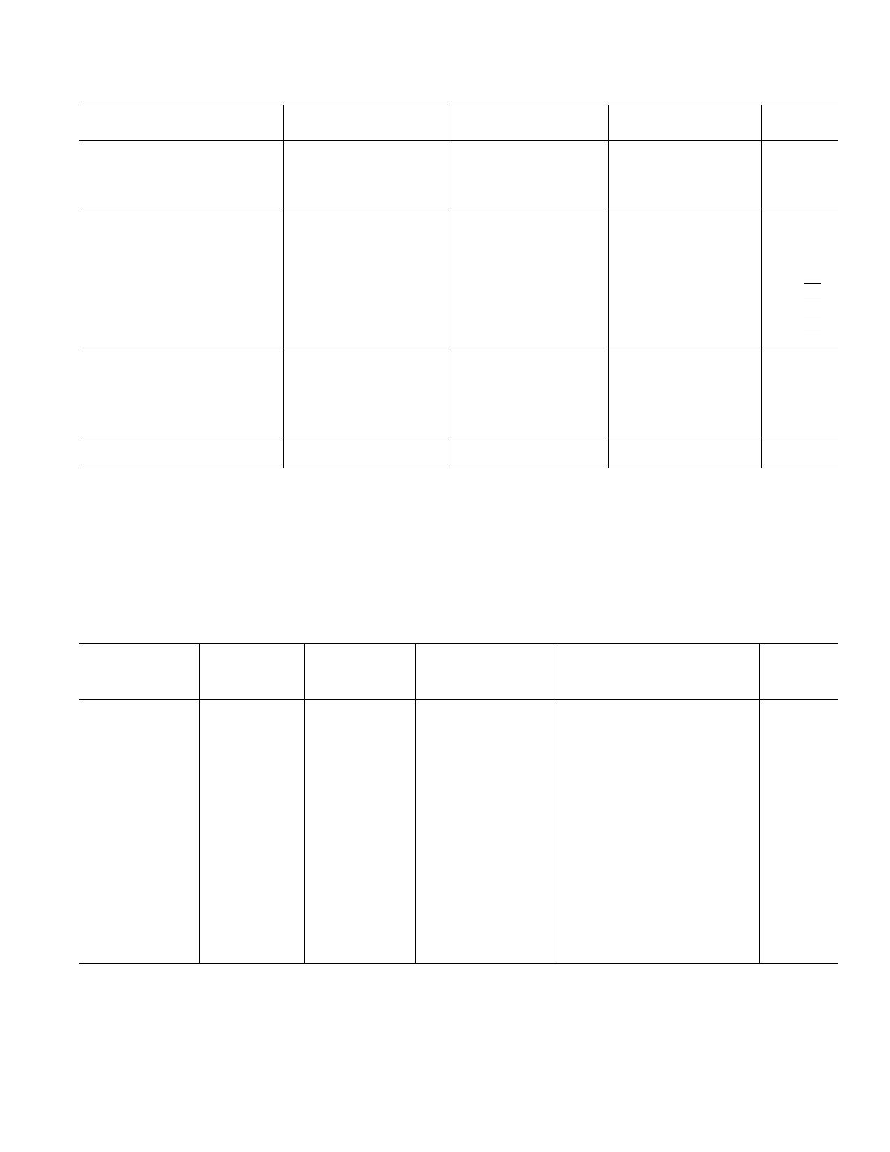
AD542/AD544/AD547
Parameter
POWER SUPPLY
Rated Performance
Operating
Quiescent Current
AD542
AD544
AD547
Min Typ Max Min Typ Max Min Typ Max Units
± 15
± 15
± 15
V
±5
±18 ± 5
±18 ± 5
±18 V
1.1 1.5
1.8 2.5
1.1 1.5 mA
VOLTAGE NOISE
0.1 Hz to 10 Hz
J Grade
K, L, S Grades
10 Hz
100 Hz
1 kHz
10 kHz
2.0
2.0
2.0
µV p-p
2.0
2.0
4.0 µV p-p
70
35
70
nV/√Hz
45
22
45
nV/√Hz
30
18
30
nV/√Hz
25
16
25
nV/√Hz
TEMPERATURE RANGE
Operating, Rated Performance
J, K, L Grades
S Grade
Storage
0 to +70
–55 to +125
–65 to +150
0 to +70
–55 to +125
–65 to +150
0 to +70
°C
–55 to +125
°C
–65 to +150
°C
TRANSISTOR COUNT
29
29
29
NOTES
1Open-Loop Gain is specified with VOS both nulled and unnulled.
2Input Offset Voltage specifications are guaranteed after 5 minutes of operation at T A = +25°C.
3Input Offset Voltage Drift is specified with the offset voltage unnulled. Nulling will induce an additional 3 µV/°C/mV of nulled offset.
4Bias Current specifications are guaranteed at either input after 5 minutes of operation at T A = +25°C. For higher temperatures, the current doubles every 10°C.
5Defined as the maximum safe voltage between inputs, such that neither exceeds ± 10 V from ground.
Specifications subject to change without notice.
Specifications shown in boldface are tested on all production units at final electrical test. Results from those tests are used to calculate outgoing quality levels.
All min and max specifications are guaranteed, although only those shown in boldface are tested on all production units.
Model
AD542JCHIPS
AD542JH
AD542KH
AD542LH
AD542SH
AD542SH/883B
AD544JH
AD544KH
AD544LH
AD544SH
AD544SH/883B
AD547JH
AD547KH
AD547LH
AD547SCHIPS
AD547SH/883B
Initial
Offset
Voltage
2.0 mV
2.0 mV
1.0 mV
0.5 mV
1.0 mV
1.0 mV
2.0 mV
1.0 mV
0.5 mV
1.0 mV
1.0 mV
1.0 mV
0.5 mV
0.25 mV
0.5 mV
0.5 mV
ORDERING GUIDE
Offset
Voltage
Drift
20 µV/°C
20 µV/°C
10 µV/°C
5 µV/°C
15 µV/°C
15 µV/°C
20 µV/°C
10 µV/°C
5 µV/°C
15 µV/°C
15 µV/°C
5 µV/°C
2 µV/°C
1 µV/°C
5 µV/°C
5 µV/°C
Settling Time
to ؎0.012% for
a 10 V Step
5 µs
5 µs
5 µs
5 µs
5 µs
5 µs
3 µs
3 µs
3 µs
3 µs
3 µs
5 µs
5 µs
5 µs
5 µs
5 µs
Package
Description
Bare Die
8-Pin Hermetic Metal Can
8-Pin Hermetic Metal Can
8-Pin Hermetic Metal Can
8-Pin Hermetic Metal Can
8-Pin Hermetic Metal Can
8-Pin Hermetic Metal Can
8-Pin Hermetic Metal Can
8-Pin Hermetic Metal Can
8-Pin Hermetic Metal Can
8-Pin Hermetic Metal Can
8-Pin Hermetic Metal Can
8-Pin Hermetic Metal Can
8-Pin Hermetic Metal Can
Bare Die
8-Pin Hermetic Metal Can
Package
Option
H-08A
H-08A
H-08A
H-08A
H-08A
H-08A
H-08A
H-08A
H-08A
H-08A
H-08A
H-08A
H-08A
H-08A
REV. B
–3–
Share Link: 