AD7150BRMZ-REEL(Rev0) View Datasheet(PDF) - Analog Devices
Part Name
Description
Manufacturer
AD7150BRMZ-REEL
(Rev.:Rev0)
(Rev.:Rev0)
Analog Devices

AD7150BRMZ-REEL Datasheet PDF : 28 Pages
| |||
AD7150
Parameter
POWER REQUIREMENTS
VDD-to-GND Voltage
IDD Current4
IDD Current Power-Down Mode4
Min
Typ
Max Unit1
2.7
3.6 V
100
120 μA
1
5
μA
3
10 μA
Test Conditions/Comments
VDD = 3.3 V, nominal
Temperature ≤ 25°C
Temperature = 85°C
1 Capacitance units: one picofarad (1 pF) = 1 × 10⁻¹² farad (F); one femtofarad (1 fF) = 10−15 farad (F).
2 The CAPDAC can be used to shift (offset) the input range. The total capacitance of the sensor can therefore be up to the sum of the CAPDAC value and the conversion
input range. With the autoCAPDAC feature, the CAPDAC is adjusted automatically when the CDC input value is lower than 25% or higher than 75% of the CDC
nominal input range.
3 Specification is not production tested but is supported by characterization data at initial product release.
4 Digital inputs equal to VDD or GND.
TIMING SPECIFICATIONS
VDD = 2.7 V to 3.6 V; GND = 0 V; Input Logic 0 = 0 V; Input Logic 1 = VDD; –40°C to +85°C, unless otherwise noted.
Table 2.
Parameter
Min Typ Max Unit Test Conditions/Comments
CONVERTER
Conversion Time
10
ms
Both channels, 5 ms per channel.
Wake-Up Time from Power-Down Mode1, 2
0.15
ms
Power-Up Time1, 3
2
ms
Reset Time1, 4
2
ms
SERIAL INTERFACE5, 6
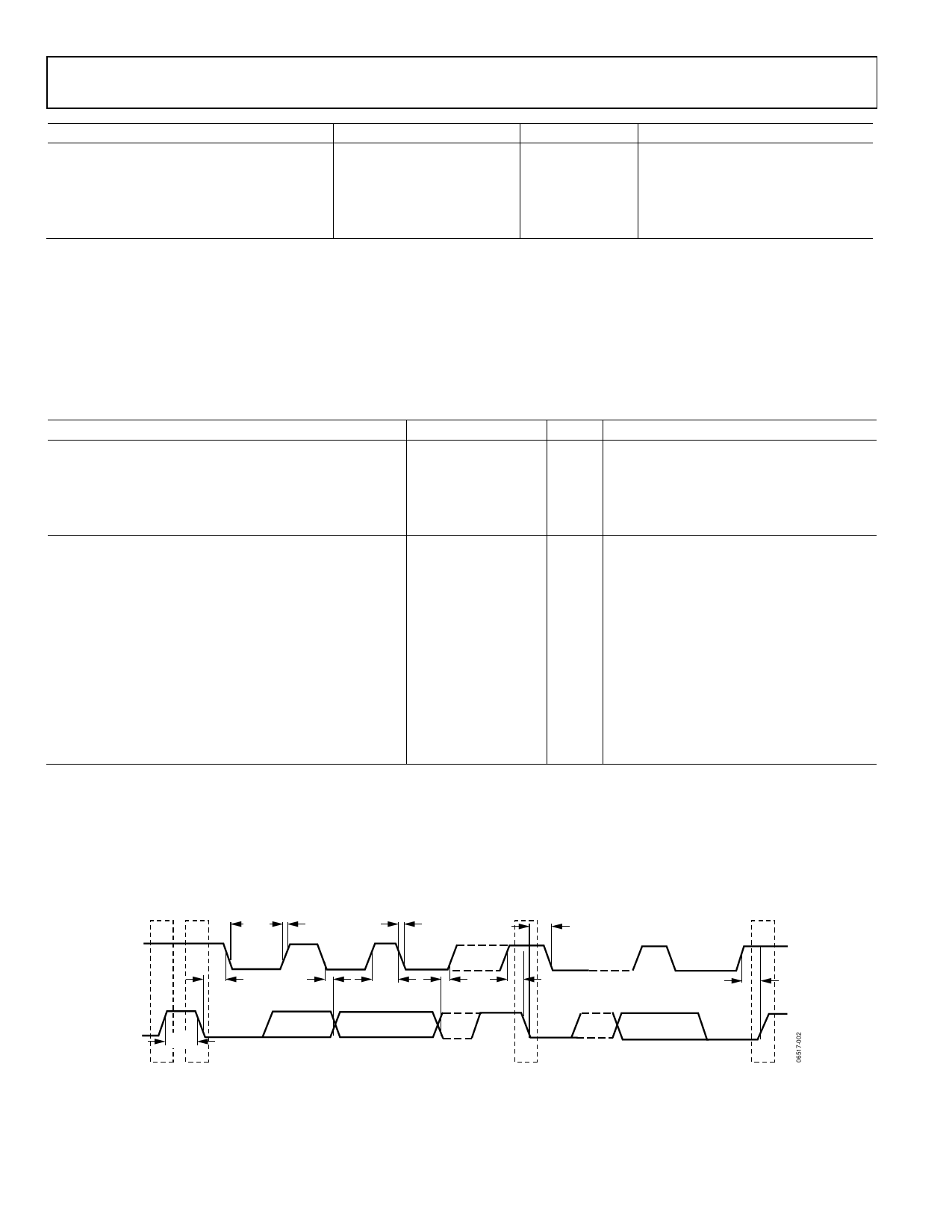
See Figure 2.
SCL Frequency
0
400 kHz
SCL High Pulse Width, tHIGH
0.6
μs
SCL Low Pulse Width, tLOW
1.3
μs
SCL, SDA Rise Time, tR
0.3
μs
SCL, SDA Fall Time, tF
0.3
μs
Hold Time (Start Condition), tHD;STA
0.6
μs
After this period, the first clock is generated.
Setup Time (Start Condition), tSU;STA
0.6
μs
Relevant for repeated start condition.
Data Setup Time, tSU;DAT
0.1
μs
Setup Time (Stop Condition), tSU;STO
0.6
μs
Data Hold Time (Master), tHD;DAT
10
ns
Bus-Free Time (Between Stop and Start Condition), tBUF 1.3
μs
1 Specification is not production tested but is supported by characterization data at initial product release.
2 Wake-up time is the maximum delay between the last SCL edge writing the configuration register and the start of conversion.
3 Power-up time is the maximum delay between the VDD crossing the minimum level (2.7 V) and either the start of conversion or when ready to receive a serial interface
command.
4 Reset time is the maximum delay between the last SCL edge writing the reset command and either the start of conversion or when ready to receive a serial interface
command.
5 Sample tested during initial release to ensure compliance.
6 All input signals are specified with input rise/fall times = 3 ns, measured between the 10% and 90% points. Timing reference points at 50% for inputs and outputs.
Output load = 10 pF.
tLOW tR
tF
tHD;STA
SCL
tHD;STA
tHD;DAT
tHIGH
tSU;DAT
tSU;STA
tSU;STO
SDA
tBUF
P
S
S
P
Figure 2. Serial Interface Timing Diagram
Rev. 0 | Page 4 of 28
Share Link: