AD7150BRMZ-REEL(Rev0) View Datasheet(PDF) - Analog Devices
Part Name
Description
Manufacturer
AD7150BRMZ-REEL
(Rev.:Rev0)
(Rev.:Rev0)
Analog Devices

AD7150BRMZ-REEL Datasheet PDF : 28 Pages
| |||
AD7150
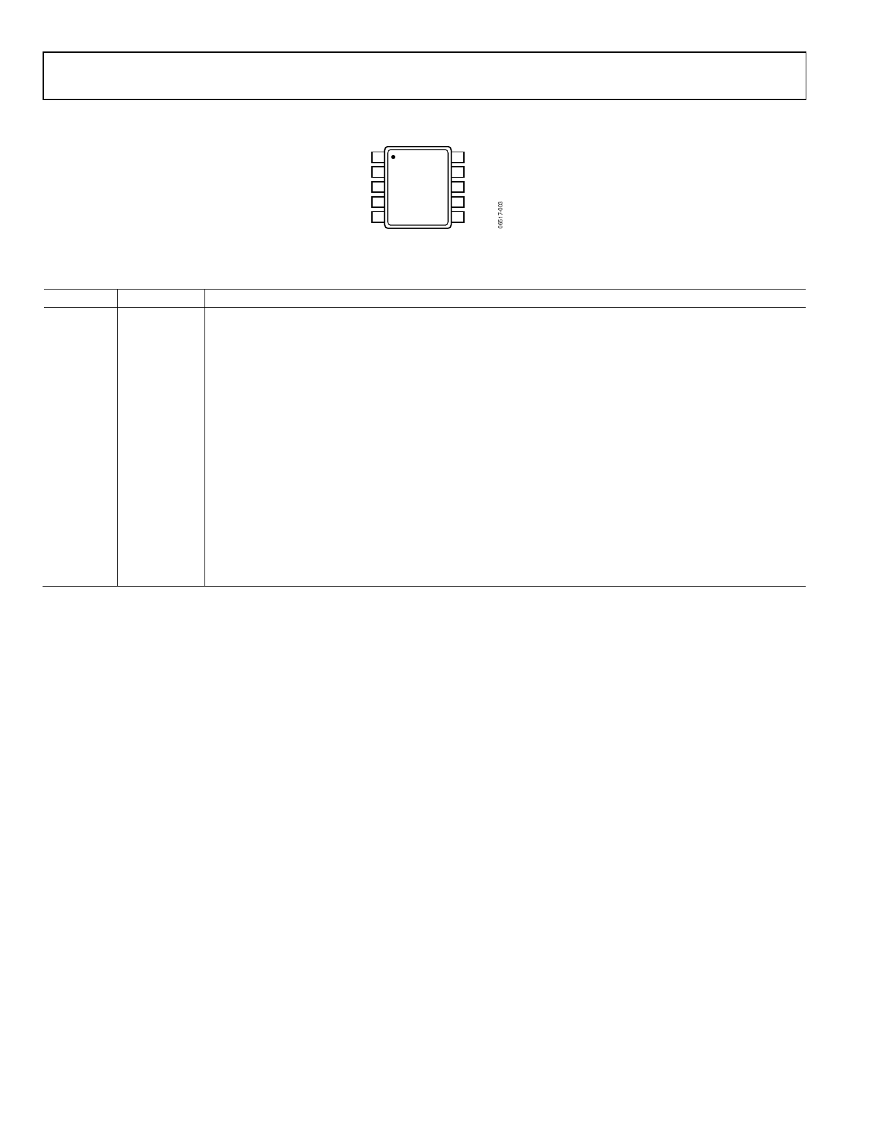
PIN CONFIGURATION AND FUNCTION DESCRIPTIONS
GND 1
VDD 2
CIN2 3
CIN1 4
EXC2 5
10 SDA
AD7150
TOP VIEW
(Not to Scale)
9 SCL
8 OUT2
7 OUT1
6 EXC1
Figure 3. Pin Configuration
Table 4. Pin Function Descriptions
Pin No.
Mnemonic Description
1
GND
Ground Pin.
2
VDD
Power Supply Voltage. This pin should be decoupled to GND using a low impedance capacitor, for example,
0.1 μF X7R multilayer ceramic.
3
CIN2
CDC Capacitive Input Channel 2. The measured capacitance (sensor) is connected between the EXC2 pin and
the CIN2 pin. If not used, this pin can be left open circuit or connected to GND.
4
CIN1
CDC Capacitive Input Channel 1. The measured capacitance (sensor) is connected between the EXC1 pin and
the CIN1 pin. If not used, this pin can be left open circuit or connected to GND.
5
EXC2
CDC Excitation Output Channel 2. The measured capacitance is connected between the EXC2 pin and the
CIN2 pin. If not used, this pin should be left as an open circuit.
6
EXC1
CDC Excitation Output Channel 1. The measured capacitance is connected between the EXC1 pin and the
CIN1 pin. If not used, this pin should be left as an open circuit.
7
OUT1
Logic Output Channel 1. A high level on this output indicates proximity detected on CIN1.
8
OUT2
Logic Output Channel 2. A high level on this output indicates proximity detected on CIN2.
9
SCL
Serial Interface Clock Input. Connects to the master clock line. Requires a pull-up resistor if not provided
elsewhere in the system.
10
SDA
Serial Interface Bidirectional Data. Connects to the master data line. Requires a pull-up resistor if not provided
elsewhere in the system.
Rev. 0 | Page 6 of 28
Share Link: