TC4426 View Datasheet(PDF) - Microchip Technology
Part Name
Description
Manufacturer
TC4426 Datasheet PDF : 20 Pages
| |||
TC4426/TC4427/TC4428
1.0 ELECTRICAL
CHARACTERISTICS
Absolute Maximum Ratings †
Supply Voltage ..................................................... +22V
Input Voltage, IN A or IN B
..................................... (VDD + 0.3V) to (GND – 5V)
Package Power Dissipation (TA ≤ 70°C)
DFN .............................................................. Note 3
MSOP .......................................................... 340 mW
PDIP ............................................................ 730 mW
SOIC............................................................ 470 mW
Storage Temperature Range.............. -65°C to +150°C
Maximum Junction Temperature ...................... +150°C
† Stresses above those listed under “Absolute Maximum
Ratings” may cause permanent damage to the device. These
are stress ratings only and functional operation of the device
at these or any other conditions above those indicated in the
operation sections of the specifications is not implied.
Exposure to Absolute Maximum Rating conditions for
extended periods may affect device reliability.
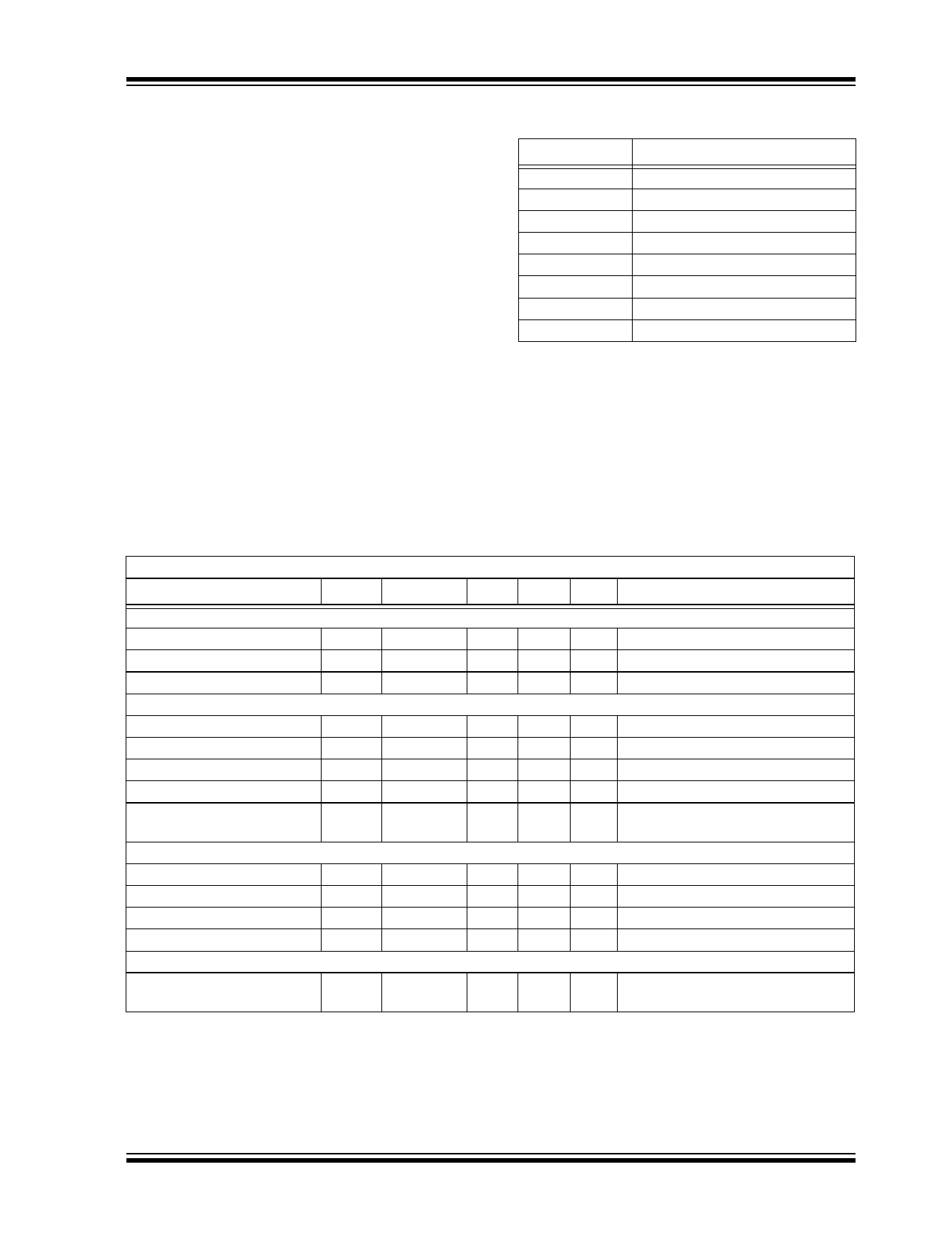
PIN FUNCTION TABLE
Name
NC
IN A
GND
IN B
OUT B
VDD
OUT A
NC
Function
No Connection
Input A
Ground
Input B
Output B
Supply Input
Output A
No Connection
DC CHARACTERISTICS
Electrical Specifications: Unless otherwise noted, TA = +25ºC with 4.5V ≤ VDD ≤ 18V.
Parameters
Sym
Min
Typ Max Units
Conditions
Input
Logic ‘1’, High Input Voltage
VIH
2.4
—
—
V Note 2
Logic ‘0’, Low Input Voltage
VIL
—
— 0.8 V
Input Current
IIN
-1.0
— +1.0 μA 0V ≤ VIN ≤ VDD
Output
High Output Voltage
Low Output Voltage
Output Resistance
Peak Output Current
Latch-Up Protection
Withstand Reverse Current
Switching Time (Note 1)
VOH
VOL
RO
IPK
IREV
VDD – 0.025
—
—
—
—
—
—
7
1.5
> 0.5
—
0.025
10
—
—
V DC Test
V DC Test
Ω IOUT = 10 mA, VDD = 18V
A VDD = 18V
A Duty cycle ≤ 2%, t ≤ 300 μs
VDD = 18V
Rise Time
Fall Time
Delay Time
Delay Time
Power Supply
tR
—
19 30 ns Figure 4-1
tF
—
19 30 ns Figure 4-1
tD1
—
20 30 ns Figure 4-1
tD2
—
40 50 ns Figure 4-1
Power Supply Current
IS
—
—
Note 1: Switching times ensured by design.
—
4.5 mA VIN = 3V (Both inputs)
— 0.4
VIN = 0V (Both inputs)
2: For V temperature range devices, the VIH (Min) limit is 2.0V.
3: Package power dissipation is dependent on the copper pad area on the PCB.
© 2006 Microchip Technology Inc.
DS21422D-page 3
Share Link: 