AD9803 View Datasheet(PDF) - Analog Devices
Part Name
Description
Manufacturer
AD9803 Datasheet PDF : 19 Pages
| |||
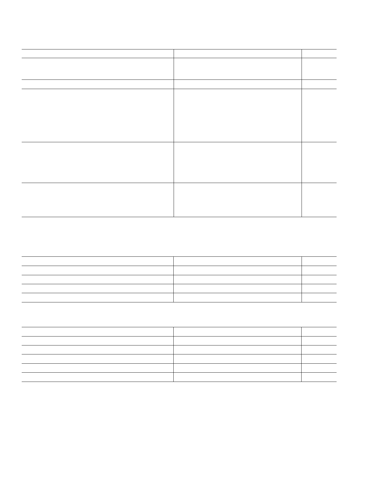
AD9803–SPECIFICATIONS
AUX-MODE SPECIFICATIONS (TMIN to TMAX, ACVDD = ADVDD = DVDD = +2.8 V, fADCCLK = 18 MHz unless otherwise noted)
Parameter
POWER CONSUMPTION
Normal (D-Reg 00)
High Speed (D-Reg 01)
MAXIMUM CLOCK RATE
PGA
Max Input Range
Max Output Range
Digital Gain Control
Gain Control Resolution
Gain (Selected by the Serial I/F)
Gain(0)
Gain(255)
ACTIVE CLAMP (CLAMP ON)
Clamp Level (Selectable by the Serial I/F)
CLP(0) (E-Reg 00)
CLP(1) (E-Reg 01)
CLP(2) (E-Reg 10)
CLP(3) (E-Reg 11)
TIMING SPECIFICATIONS1
Pipeline Delay
Internal Clock Delay (tID)
Output Delay (tOD)
Output Hold Time (tHOLD)
NOTES
120 pF loading; timing shown in Figure 2.
Specifications subject to change without notice.
Min
18
700
1000
2
Typ
Max
80
110
8 (Fixed)
–3.5
10.5
34
50
66
18
4 (Fixed)
5
20
Units
mW
mW
MHz
mV p-p
mV p-p
Bits
dB
dB
LSB
LSB
LSB
LSB
Cycles
ns
ns
ns
ADC-MODE SPECIFICATIONS (TMIN to TMAX, ACVDD = ADVDD = DVDD = +2.8 V, fADCCLK = 18 MHz unless otherwise noted)
Parameter
Min
Typ
Max
Units
POWER CONSUMPTION (Normal D-Reg 00)
MAXIMUM CLOCK RATE
65
18
mW
MHz
ACTIVE CLAMP (Same as AUX-MODE)
TIMING SPECIFICATIONS (Same as AUX-MODE)
Specifications subject to change without notice.
DAC SPECIFICATIONS (DAC1 and DAC2)
Parameter
RESOLUTION
MIN OUTPUT
MAX OUTPUT
MAX CURRENT LOAD
MAX CAPACITIVE LOAD
Specifications subject to change without notice.
Min
Typ
Max
8 (Fixed)
0.1
VDD – 0.1
1
500
Units
Bits
V
V
mA
pF
–4–
REV. 0
Share Link: 