AD9845B(RevA) View Datasheet(PDF) - Analog Devices
Part Name
Description
Manufacturer
AD9845B Datasheet PDF : 24 Pages
| |||
AD9845B
DEFINITIONS OF SPECIFICATIONS
Differential Nonlinearity (DNL)
An ideal ADC exhibits code transitions that are exactly 1 LSB
apart. DNL is the deviation from this ideal value. Thus, every code
must have a finite width. No missing codes guaranteed to 12-bit
resolution indicates that all 4096 codes, must be present over
all operating conditions.
Peak Nonlinearity
Peak nonlinearity, a full signal chain specification, refers to
the peak deviation of the output of the AD9845B from a true
straight line. The point used as “zero scale” occurs 1/2 LSB
before the first code transition. “Positive full scale” is defined as a
Level 1, 1/2 LSB beyond the last code transition. The deviation is
measured from the middle of each particular output code to the
true straight line. The error is then expressed as a percentage of the
2 V ADC full-scale signal. The input signal is always appropriately
gained up to fill the ADC’s full-scale range.
Total Output Noise
The rms output noise is measured using histogram techniques.
The standard deviation of the ADC output codes is calculated
in LSB and represents the rms noise level of the total signal
chain at the specified gain setting. The output noise can be
converted to an equivalent voltage using the relationship
1 LSB = (ADC Full Scale/2N codes)
where N is the bit resolution of the ADC. For the AD9845B,
1 LSB is approximately 488 mV.
Power Supply Rejection (PSR)
The PSR is measured with a step change applied to the supply
pins. This represents a high frequency disturbance on the
AD9845B’s power supply. The PSR specification is calculated
from the change in the data outputs for a given step change in
the supply voltage.
Internal Delay for SHP/SHD
The internal delay (also called aperture delay) is the time delay
that occurs from when a sampling edge is applied to the AD9845B
until the actual sample of the input signal is held. Both SHP and
SHD sample the input signal during the transition from low to
high, so the internal delay is measured from each clock’s rising
edge to the instant the actual internal sample is taken.
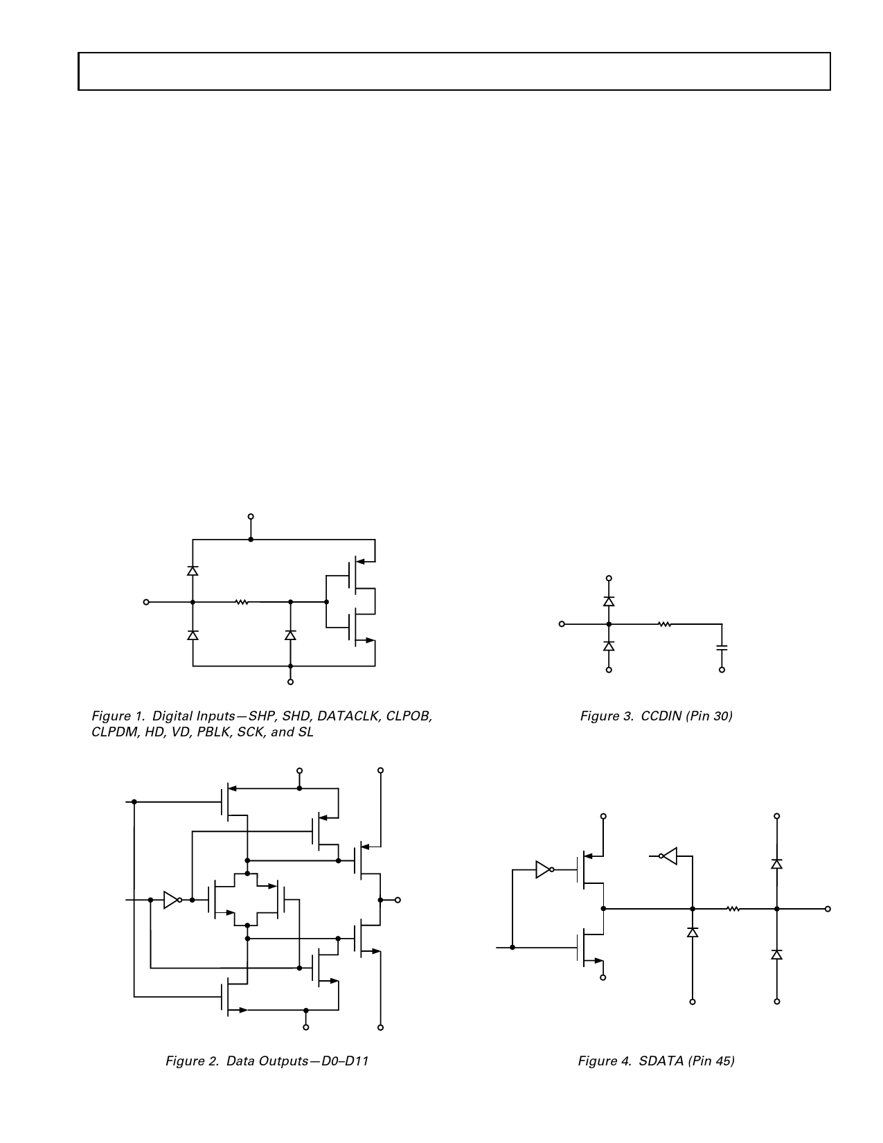
EQUIVALENT INPUT CIRCUITS
DVDD
330⍀
AVDD
DVSS
Figure 1. Digital Inputs—SHP, SHD, DATACLK, CLPOB,
CLPDM, HD, VD, PBLK, SCK, and SL
DVDD
DRVDD
DATA
THREE-
STATE
DOUT
RNW
DVSS
DRVSS
Figure 2. Data Outputs—D0–D11
REV. A
–7–
AVSS
ACVSS
Figure 3. CCDIN (Pin 30)
DVDD
DATA IN
DATA OUT
DVDD
330⍀
DVSS
DVSS
DVSS
Figure 4. SDATA (Pin 45)
Share Link: 