ADC0808S125 View Datasheet(PDF) - Integrated Device Technology
Part Name
Description
Manufacturer
ADC0808S125 Datasheet PDF : 22 Pages
| |||
Integrated Device Technology
ADC0808S125/250
Single 8-bit ADC, up to 125 MHz or 250 MHz
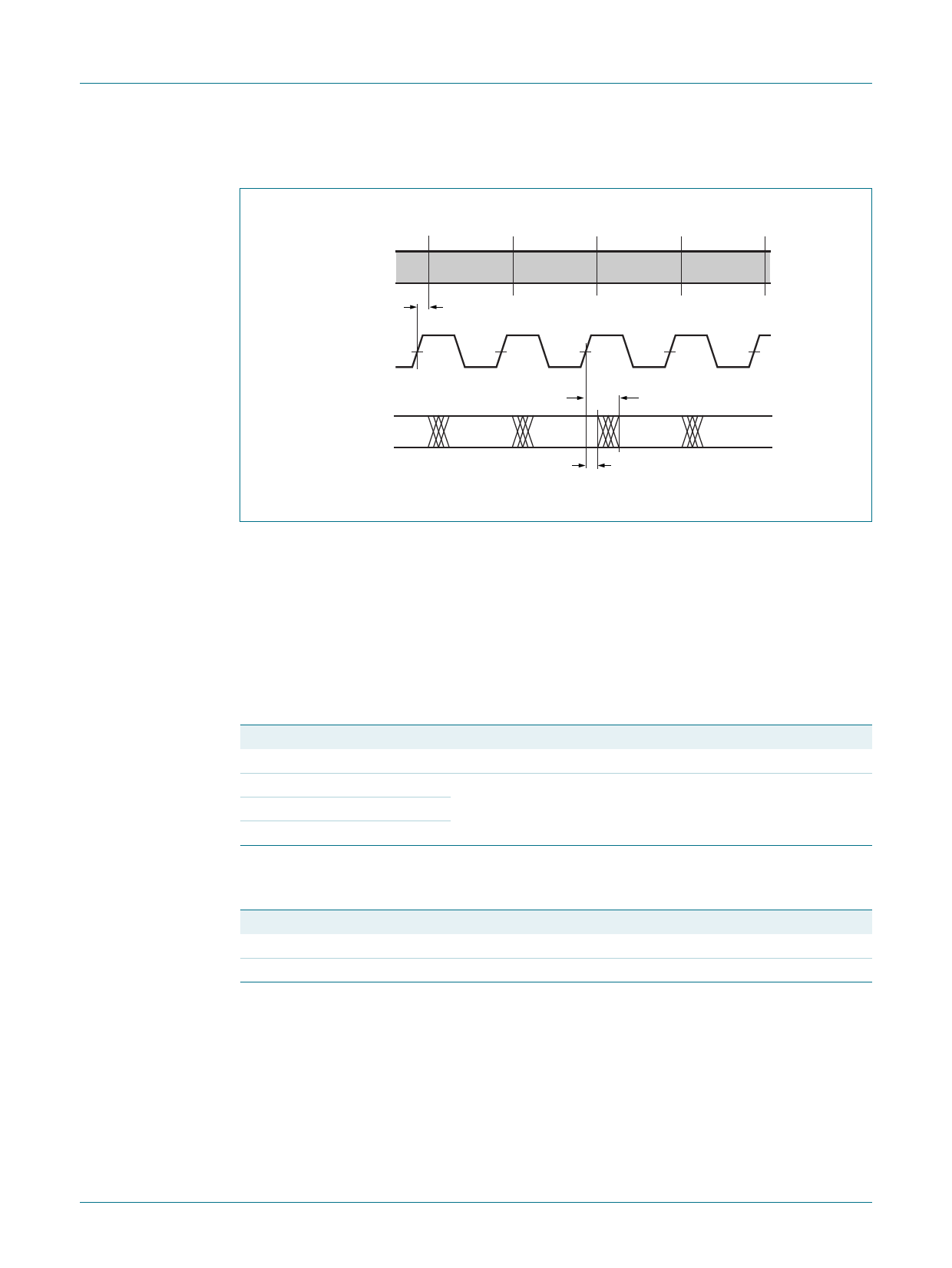
7.3 Timing output
sample
n
IN, INN
sample
n+1
td(s)
CLK+, CLK−
n
sample
n+2
sample
n+3
sample
n+4
50 %
D0 to D7
data
n−2
td(o)
data
data
n−1
n
th(o)
Fig 5. Output timing diagram (CCS not selected)
data
n+1
001aab892
7.4 Timing complete conversion signal
The ADC0808S generates an adjustable clock output signal on pin CCS called Complete
Conversion Signal, which can be used to control the acquisition of converted output data
to the digital circuit connected to the ADC0808S output data bus.
Two logic input pins DEL0 and DEL1 control the delay of the edge of the CCS signal to
achieve an optimal position in the stable, usable zone of the data as shown in Figure 6.
Table 7. Complete conversion signal selection
Pin DEL0
Pin DEL1
Pin CCS
LOW
LOW
high-impedance
HIGH
LOW
active; see Table 13
LOW
HIGH
HIGH
HIGH
Pin CCSSEL selects the CCS frequency; see Table 8.
Table 8. Complete conversion signal frequency selection
Pin CCSSEL
HIGH or not connected
CCS frequency (fCCS)
fclk
LOW
fclk / 2
ADC0808S125_ADC0808S250_4
Product data sheet
Rev. 04 — 2 July 2012
© IDT 2012. All rights reserved.
7 of 22
Share Link: 