ADD8708WCPZ-REEL7 View Datasheet(PDF) - Analog Devices
Part Name
Description
Manufacturer
ADD8708WCPZ-REEL7 Datasheet PDF : 16 Pages
| |||
ADD8708
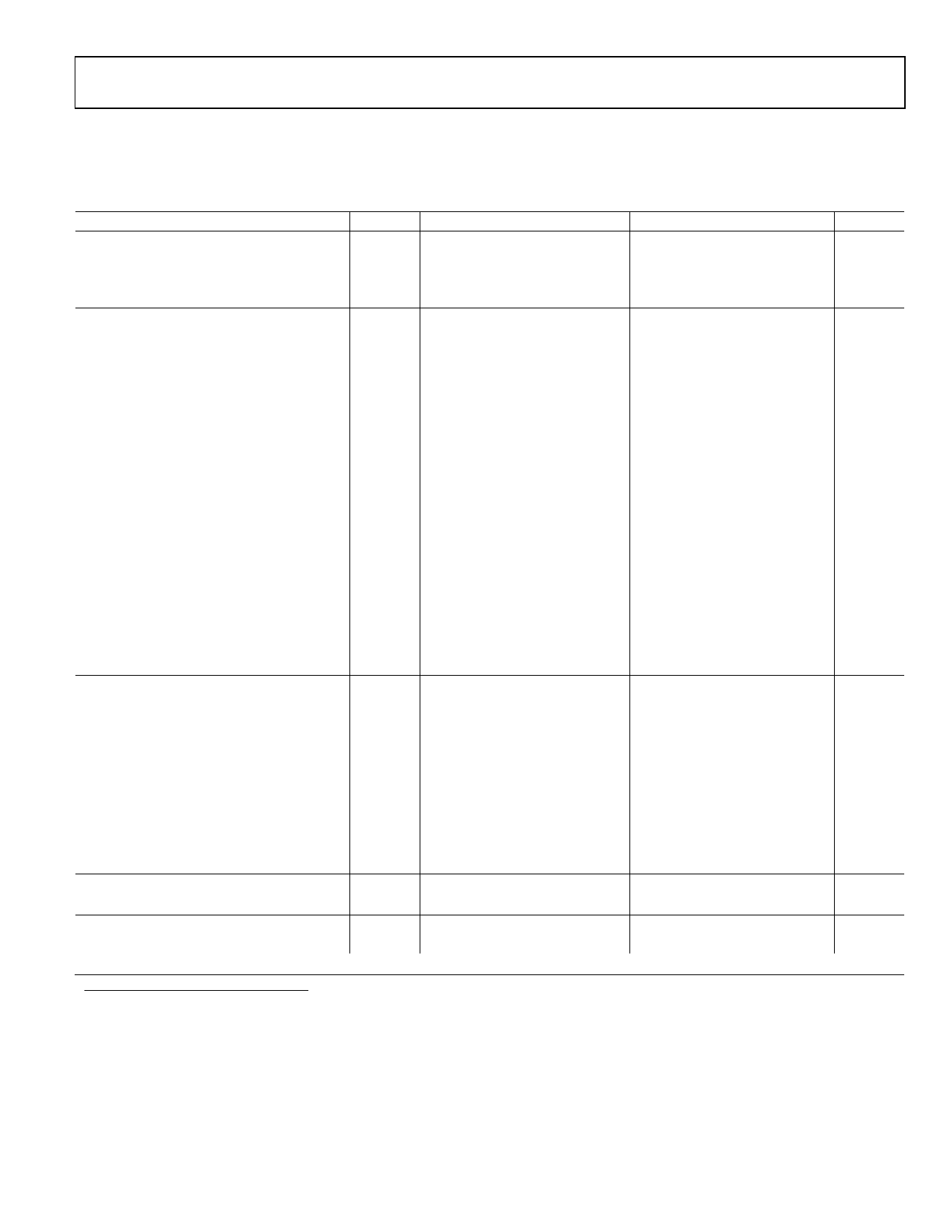
ELECTRICAL CHARACTERISTICS
VDD = 16 V, TA @ 25°C, unless otherwise noted.
Table 1.
Parameter
Symbol Conditions
Min
Typ
Max
Unit
GAMMA CURVE CHARACTERISTICS
Accuracy
RACC1
0.1
0.4
%
Programming Resolution
RRES
500 segments
0.2
%
Total Resistor String
RTOTAL
15
kΩ
BUFFER CHARACTERISTICS
OUTPUTS
Output Voltage Range (Ch18 to Ch10) VOUT
IL = 100 µA
1.4
VDD
V
Output Voltage Range (Ch9 to Ch1)
VOUT
IL = 100 µA
0
VDD − 1.4 V
Output vs. Load (Ch18, Ch17, Ch2, Ch1) ∆VOUT2
Output vs. Load (Ch16 to Ch3)
∆VOUT2
IL = 20 mA
IL = 5 mA
15
mV
5
mV
INPUTS
Offset Voltage
VOS
5
15
mV
Offset Voltage Drift
∆VOS/∆T −40°C ≤ TA ≤ +105°C
20
µV/°C
Input Bias Current
IB
−40°C ≤ TA ≤ +105°C
0.5
1.5
µA
Input Voltage Range (Ch18 to Ch10)
VIN
1.4
VDD
V
Input Voltage Range (Ch9 to Ch1)
VIN
0
VDD − 1.4 V
DYNAMIC PERFORMANCE
Slew Rate
SR
RL = 10 kΩ, CL = 200 pF
4
6
V/µs
Bandwidth
BW
–3 dB, RL = 10 kΩ, CL = 200 pF
4.5
MHz
Settling Time to 0.1%
tS
1 V, RL = 10 kΩ, CL = 200 pF
1.1
µs
Phase Margin
Фo
RL = 10 kΩ, CL = 200 pF
55
Degrees
Power Supply Rejection Ratio
PSRR
VDD = 7 V to 17 V,
68
90
dB
−40°C ≤ TA ≤ +105°C
VOLTAGE REGULATOR
Programmable Range
VREG OUT
5
VDD − 0.6 V
Initial Regulator Accuracy
VACC
No load; VREG OUT = 14.4V
0.4
1.5
%
Dropout Voltage
VDO
IL = 100 µA
100
150
mV
IL = 5 mA
310
350
mV
Line Regulation
REGLINE VIN = 8.5 V to 16.5 V, VOUT = 8 V
0.01
0.20
%/V
Load Regulation
REGLOAD IO = 100 µA to 10 mA
0.02
0.10
%/mA
Maximum Load Current
IO
−40°C ≤ TA ≤ +105°C
5
mA
Feedback Reference Voltage
VREF
1.2
V
Feedback Input Bias Current
IB FB
−40°C ≤ TA ≤ +105°C
-150
10
150
nA
SYSTEM ACCURACY
Total Error3, 4
VTotal Error −40°C ≤ TA ≤ +105°C
0.5
3
%
POWER SUPPLY
Supply Voltage
VDD
7.5
16
V
Supply Current
ISY
No load; −40°C ≤ TA ≤ +105°C
9.5
16
mA
1 Gamma curve accuracy includes resistor matching and buffer errors, but excludes the regulator error.
2 ∆VOUT is the shift from the desired output voltage under the specified current load.
3 Total error is the difference between the designed and actual output voltage divided by the actual regulator output voltage or full-scale voltage.
4 Total error includes regulator error, resistor string error, bias current effects, and buffer offset voltage.
Rev. 0 | Page 3 of 16
Share Link: 