ADF4150BCPZ-RL7 View Datasheet(PDF) - Analog Devices
Part Name
Description
Manufacturer
ADF4150BCPZ-RL7 Datasheet PDF : 28 Pages
| |||
Data Sheet
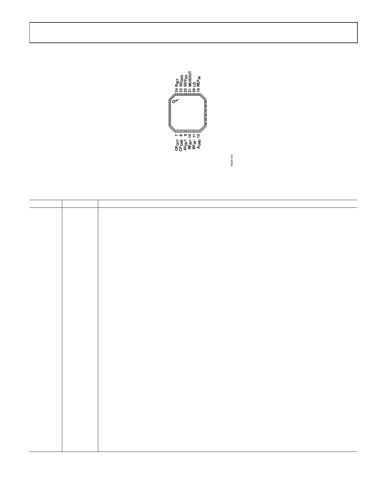
PIN CONFIGURATION AND FUNCTION DESCRIPTIONS
ADF4150
CLK 1
DATA 2
LE 3
CE 4
SW 5
VP 6
PIN 1
INDICATOR
ADF4150
TOP VIEW
(Not to Scale)
18 DVDD
17 PDBRF
16 AVDD2
15 RFOUT+
14 RFOUT−
13 AGND
NOTES
1. THE LFCSP HAS AN EXPOSED PADDLE
THAT MUST BE CONNECTED TO GND.
Figure 3. Pin Configuration
Table 4. Pin Function Descriptions
Pin No.
Mnemonic Description
1
CLK
Serial Clock Input. Data is clocked into the 32-bit shift register on the CLK rising edge. This input is a high
impedance CMOS input.
2
DATA
Serial Data Input. The serial data is loaded MSB first with the three LSBs as the control bits. This input is a high
impedance CMOS input.
3
LE
Load Enable, CMOS Input. When LE goes high, the data stored in the shift register is loaded into the register
that is selected by the three LSBs.
4
CE
Chip Enable. A logic low on this pin powers down the device and puts the charge pump into three-state
mode. Taking the pin high powers up the device depending on the status of the power-down bits.
5
SW
Fastlock Switch. Make a connection to this pin from the loop filter when using the fastlock mode.
6
VP
Charge Pump Power Supply. This pin should be greater than or equal to AVDD. In systems where AVDD is 3 V, it
can be set to 5.5 V and used to drive a VCO with a tuning range of up to 5.5 V.
7
CPOUT
Charge Pump Output. When enabled, this provides ±ICP to the external loop filter. The output of the loop filter
is connected to VTUNE to drive the external VCO.
8
CPGND
Charge Pump Ground. This is the ground return pin for CPOUT.
9
AVDD1
Analog Power Supply. This pin ranges from 3.0 V to 3.6 V. Decoupling capacitors to the analog ground plane
are to be placed as close as possible to this pin. AVDD must have the same value as DVDD.
10
RFIN+
Input to the RF Input. This small signal input is ac-coupled to the external VCO.
11
RFIN−
Complementary Input to the RF Input. This point must be decoupled to the ground plane with a small bypass
capacitor, typically 100 pF.
12, 13
AGND
Analog Ground. This is a ground return pin for AVDD1 and AVDD2.
14
RFOUT−
Complementary RF Output. The output level is programmable. The VCO fundamental output or a divided
down version is available.
15
RFOUT+
RF Output. The output level is programmable. The VCO fundamental output or a divided down version is
available.
16
AVDD2
Analog Power Supply. This pin ranges from 3.0 V to 3.6 V. Decoupling capacitors to the analog ground plane
are to be placed as close as possible to this pin. AVDD2 must have the same value as DVDD.
17
PDBRF
RF Power-Down. A logic low on this pin mutes the RF outputs. This function is also software controllable.
18
DVDD
Digital Power Supply. This pin should be the same voltage as AVDD. Place decoupling capacitors to the ground
plane as close as possible to this pin.
19
REFIN
Reference Input. This is a CMOS input with a nominal threshold of VDD/2 and a dc equivalent input resistance
of 100 kΩ. This input can be driven from a TTL or CMOS crystal oscillator, or it can be ac-coupled.
20
LD
Lock Detect Output Pin. This pin outputs a logic high to indicate PLL lock; a logic low output indicates loss of
PLL lock.
21
MUXOUT
Multiplexer Output. This multiplexer output allows either the lock detect, the scaled RF, or the scaled reference
frequency to be accessed externally.
Rev. A | Page 7 of 28
Share Link: 