ADF7020-1 View Datasheet(PDF) - Analog Devices
Part Name
Description
Manufacturer
ADF7020-1 Datasheet PDF : 48 Pages
| |||
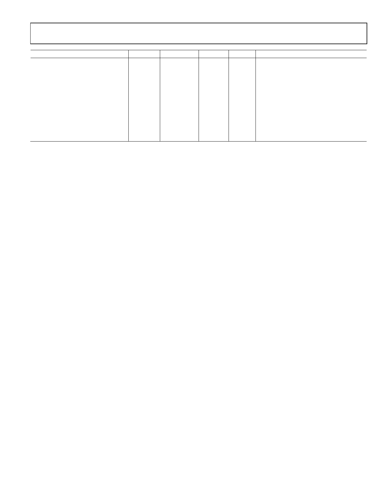
ADF7020-1
Parameter
Min
POWER SUPPLIES
Voltage Supply
VDD
2.3
Transmit Current Consumption
433 MHz, 0 dBm/5 dBm/10 dBm
Receive Current Consumption
Low Current Mode
High Sensitivity Mode
Power-Down Mode
Low Power Sleep Mode
Typ
Max
Unit
Test Conditions
3.6
13/16/21
17.6
20.1
0.1
1
V
All VDD pins must be tied together
FRF = 315 MHz, VDD = 3.0 V, PA is matched
to 50 Ω
mA
VCO_BIAS_SETTING = 2
mA
VCO_BIAS_SETTING = 2
mA
VCO_BIAS_SETTING = 2
μA
1 Higher data rates are achievable, depending on local regulations.
2 For definition of frequency deviation, see the Register 2—Transmit Modulation Register (FSK Mode) section.
3 For definition of GFSK frequency deviation, see the Register 2—Transmit Modulation Register (GFSK/GOOK Mode) section.
4 Measured as maximum unmodulated power. Output power varies with both supply and temperature.
5 For matching details, see the LNA/PA Matching section.
6 Sensitivity for combined matching network case is typically 2 dB less than separate matching networks. See Table 11 for sensitivity values at various data rates and
frequencies.
7 See Table 6 for a description of different receiver modes.
8 Follow the matching and layout guidelines to achieve the relevant FCC/ETSI specifications.
9 This figure can be used to calculate the in-band phase noise for any operating frequency. Use the following equation to calculate the in-band phase noise
performance as seen at the PA output: –198 + 10 log(fPFD) + 20 log N.
Rev. 0 | Page 7 of 48
Share Link: 